


 Dan’s Biz Bookshelf: Four Important Books You Need to Read (Not Just Say You Have)
 The Marketing Minute: Cracking the Code of Technical Marketing


A Faster Future: Graphene Based Optoelectronics
July 8, 2016 | University of CambridgeEstimated reading time: 3 minutes
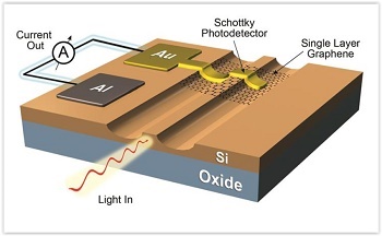
As an important step towards graphene integration in silicon photonics, researchers from the Graphene Flagship have published a paper which shows how graphene can provide a simple solution for silicon photodetection in the telecommunication wavelengths. Published in Nano Letters, this exciting research is a collaboration between the University of Cambridge (UK), The Hebrew University (Israel) and John Hopkins University (USA).
The mission of the Graphene Flagship is to translate graphene out of the academic laboratory, through industry and into society. This broad and ambitious aim has been at the forefront of the choices made to direct the Flagship; it focuses on real problem areas where it can make a real difference such as in Optical Communications.
Optical Communications are increasingly important because they have the potential to solve one of the biggest problems of our information age: energy consumption. Almost everything we do in everyday life consumes information and all of this information is powered by energy. If we want more and more information, we need more and more energy. In the near future, the major consumers of data traffic will be machine-to-machine communication and the Internet of Things (IoT).
To enable the IoT and the level of information it requires, current silicon photonics has a problem: it needs ten times more energy than we can provide. So, if we want this new, improved internet age, new technological, power-efficient solutions need to be found. This is why the drive to graphene-based optical communication is so important.
Over the last few years, optical communications have increased their viability over standard metal-based electronic interconnects. The current silicon-based photodetector used in optical communications has a major issue when it comes to detecting data in the near infrared range, which is the range used for telecommunications. The telecom industry has overcome this problem by integrating germanium absorbers with the standard silicon photonic devices. They have been able to make fully functioning devices on chips using this process. However, this process is complex.
In the new paper, graphene is interfaced with silicon on chip to make high responsivity Schottky barrier photodetectors. These graphene-based photodetectors achieve 0.37A/W responsivity at 1.55μm using avalanche multiplication. This high responsivity is comparable to that of the Silicon Germanium detectors currently used in silicon photonics.
Prof. Andrea Ferrari from the Cambridge Graphene Centre, who is also the Science and Technology Officer and the Chair of the Management Panel for the Graphene Flagship stated; “This is a significant result which proves that graphene can compete with the current state of the art by producing devices that can be made more simply, cheaply and work at different wavelengths. Thus paving the way for graphene integrated silicon photonics.”
Dr Ilya Goykhman, from the University of Cambridge, and the paper's lead author, said; “The vision here is for graphene to play an important part in enabling optical communication technologies. This is a first step towards this, and, over the next two years the aim of the wafer-scale integration and optoelectronics work-packages of the Flagship is to really make this happen”.
Talking further about the Graphene Flagship and its collaborative approach to research, Prof Ferrari commented “Graphene can beat current silicon photonic technology in terms of energy consumption. The Graphene Flagship is investing a lot of resources into wafer-scale integration with the creation of a new Work Package. We have identified a vision, where graphene is the backbone for data communication, and we plan to have a telecommunication bank capable of transferring 4x28 GB/s by 2018. The research in this Nano Letters paper is the first step towards achieving that vision, the importance of which is clearly recognised by companies such as Ericsson and Alcatel-Lucent who have joined the Flagship to help develop it.”
“We have shown the potential for the detector but we also need to produce a graphene-based modulator to have a full, low energy optical telecommunication system and the Flagship is working hard on this problem. The Flagship has collected the right people in the right place at the right time to work together towards this goal. Europe will be at the cutting edge of this technology. It is a great challenge, and a great opportunity for Europe, as there is such high added value to the devices it will be cost effective to manufacture the device in Europe - keeping the value of the technology within the European community,” said Prof. Ferrari.
Share on:


Testimonial
"The I-Connect007 team is outstanding—kind, responsive, and a true marketing partner. Their design team created fresh, eye-catching ads, and their editorial support polished our content to let our brand shine. Thank you all! "
Sweeney Ng - CEE PCBSuggested Items
Meet the Author Podcast: Martyn Gaudion Unpacks the Secrets of High-Speed PCB Design
07/16/2025 | I-Connect007In this special Meet the Author episode of the On the Line with… podcast, Nolan Johnson sits down with Martyn Gaudion, signal integrity expert, managing director of Polar Instruments, and three-time author in I-Connect007’s popular The Printed Circuit Designer’s Guide to... series.
Intervala Hosts Employee Car and Motorcycle Show, Benefit Nonprofits
08/27/2024 | IntervalaIntervala hosted an employee car and motorcycle show, aptly named the Vala-Cruise and it was a roaring success! Employees had the chance to show off their prized wheels, and it was incredible to see the variety and passion on display.
KIC Honored with IPC Recognition for 25 Years of Membership and Contributions to Electronics Manufacturing Industry
06/24/2024 | KICKIC, a renowned pioneer in thermal process and temperature measurement solutions for electronics manufacturing, is proud to announce that it has been recognized by IPC for 25 years of membership and significant contributions to electronics manufacturing.
Boeing Starliner Spacecraft Completes Successful Crewed Docking with International Space Station
06/07/2024 | BoeingNASA astronauts Barry "Butch" Wilmore and Sunita "Suni" Williams successfully docked Boeing's Starliner spacecraft to the International Space Station (ISS), about 26 hours after launching from Cape Canaveral Space Force Station.
KIC’s Miles Moreau to Present Profiling Basics and Best Practices at SMTA Wisconsin Chapter PCBA Profile Workshop
01/25/2024 | KICKIC, a renowned pioneer in thermal process and temperature measurement solutions for electronics manufacturing, announces that Miles Moreau, General Manager, will be a featured speaker at the SMTA Wisconsin Chapter In-Person PCBA Profile Workshop.