


 The Right Approach: The Pros and Cons of PCB Vertical Integration
 American Made Advocacy: PCBAA’s Fifth Annual Meeting—Growing Membership and Valuable Relationships
 It's Only Common Sense: Why the Best Years of Electronics Are Still Ahead of Us


Nanoscale “rivets” give graphene qualities that may speed the wonder material’s adoption in products like flexible, transparent electronics, according to researchers at Rice University.
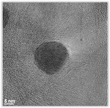
A single “rivet,” a carbon-wrapped nanoparticle of iron, attached to graphene that has been reinforced by an interconnected web of carbon nanotubes, which are also visible in this transmission electron microscope image. Courtesy of the Tour Group
The Rice lab of chemist James Tour reported the creation of “rivet graphene,” two-dimensional carbon that incorporates carbon nanotubes for strength and carbon spheres that encase iron nanoparticles, which enhance both the material’s portability and its electronic properties.
The material is the subject of a paper in the American Chemical Society journal ACS Nano.
Until now, researchers have had to transfer graphene grown via chemical vapor deposition with a polymer layer to keep it from wrinkling or ripping. But the polymer tended to leave contaminants behind and degrade graphene’s abilities to carry a current.
“Rivet graphene proved tough enough to eliminate the intermediate polymer step,” Tour said. “Also, the rivets make interfacing with electrodes far better compared with normal graphene’s interface, since the junctions are more electrically efficient.
Rivet graphene (outlined in yellow) is nearly as transparent as pure graphene and retains its strength and conductivity even when flexed. Courtesy of the Tour Group
“Finally, the nanotubes give the graphene an overall higher conductivity. So if you want to use graphene in electronic devices, this is an all-around superior material,” he said.
Tests proved rivet graphene retained the strength of the Tour lab’s rebar graphene (which incorporates nanotube reinforcement) as well as rebar’s ability to float on water. But the rivets also enhanced the material’s ability to transfer current between electrodes and the graphene, even when bent, the researchers reported.
The rivets are layers of carbon wrapped around a 30-nanometer iron core, dubbed “nano-onions” by the lab. The structures are grown in place in the CVD furnace after the dispersal of nanotubes and deposition of graphene. A final step welds all the elements together, Tour said.
Iron nanoparticles wrapped in carbon and embedded in graphene enhance the material’s connection to an electrode. Courtesy of the Tour Group
Rivet graphene is transparent enough for flexible and transparent electronics, he said, and the simplified process should be scalable.
Xinlu Li, a former visiting researcher at Rice and a professor at Chongqing University, China, is lead author of the paper. Co-authors are graduate student Junwei Sha of Rice, Tianjin University, China, and the Collaborative Innovation Center of Chemical Science and Engineering in Tianjin; graduate student Yilun Li, postdoctoral researcher Yongsung Ji and former postdoctoral researcher Seoung-Ki Lee of Rice; and Yujie Zhao of Chongqing. Tour is the T.T. and W.F. Chao Professor of Chemistry as well as a professor of computer science and of materials science and nanoengineering.
The research was funded by the Air Force Office of Scientific Research and its Multidisciplinary University Research Initiative, the Natural Science Foundation Project of China’s Chongqing Science and Technology Commission and the China Scholarship Council.


