


 Dan’s Biz Bookshelf: Four Important Books You Need to Read (Not Just Say You Have)
 The Marketing Minute: Cracking the Code of Technical Marketing


Smallest Hard Disk to Date Writes Information Atom by Atom
July 19, 2016 | TU DelftEstimated reading time: 3 minutes
Every day, modern society creates more than a billion gigabytes of new data. To store all this data, it is increasingly important that each single bit occupies as little space as possible. A team of scientists at the Kavli Institute of Nanoscience at Delft University managed to bring this reduction to the ultimate limit: they built a memory of 1 kilobyte (8,000 bits), where each bit is represented by the position of one single chlorine atom. “In theory, this storage density would allow all books ever created by humans to be written on a single post stamp”, says lead-scientist Sander Otte. They reached a storage density of 500 Terabits per square inch (Tbpsi), 500 times better than the best commercial hard disk currently available. His team reports on this memory in Nature Nanotechnology on Monday July 18.
Feynman
In 1959, physicist Richard Feynman challenged his colleagues to engineer the world at the smallest possible scale. In his famous lecture There’s Plenty of Room at the Bottom, he speculated that if we had a platform allowing us to arrange individual atoms in an exact orderly pattern, it would be possible to store one piece of information per atom. To honor the visionary Feynman, Otte and his team now coded a section of Feynman’s lecture on an area 100 nanometers wide.
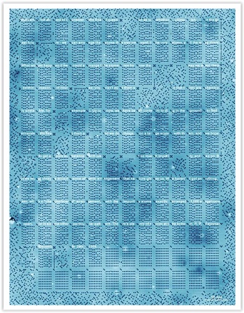
STM scan (96 nm wide, 126 nm tall) of the 1 kB memory, written to a section of Feynman’s lecture There’s Plenty of Room at the Bottom (with text markup).
Sliding puzzle
The team used a scanning tunneling microscope (STM), in which a sharp needle probes the atoms of a surface, one by one. With these probes scientists cannot only see the atoms but they can also use them to push the atoms around. “You could compare it to a sliding puzzle”, Otte explains. “Every bit consists of two positions on a surface of copper atoms, and one chlorine atom that we can slide back and forth between these two positions. If the chlorine atom is in the top position, there is a hole beneath it -- we call this a 1. If the hole is in the top position and the chlorine atom is therefore on the bottom, then the bit is a 0.” Because the chlorine atoms are surrounded by other chlorine atoms, except near the holes, they keep each other in place. That is why this method with holes is much more stable than methods with loose atoms and more suitable for data storage.
Codes
The researchers from Delft organized their memory in blocks of 8 bytes (64 bits). Each block has a marker, made of the same type of ‘holes’ as the raster of chlorine atoms. Inspired by the pixelated square barcodes (QR codes) often used to scan tickets for airplanes and concerts, these markers work like miniature QR codes that carry information about the precise location of the block on the copper layer. The code will also indicate if a block is damaged, for instance due to some local contaminant or an error in the surface. This allows the memory to be scaled up easily to very big sizes, even if the copper surface is not entirely perfect.
Datacenters
The new approach offers excellent prospects in terms of stability and scalability. Still, this type of memory should not be expected in datacenters soon. Otte: “In its current form the memory can operate only in very clean vacuum conditions and at liquid nitrogen temperature (77 K), so the actual storage of data on an atomic scale is still some way off. But through this achievement we have certainly come a big step closer”.
This research was made possible through support from the Netherlands Organisation for Scientific Research (NOW/FOM). Scientists of the International Iberian Nanotechnology Laboratory (INL) in Portugal performed calculations on the behavior of the chlorine atoms.
Share on:


Testimonial
"Advertising in PCB007 Magazine has been a great way to showcase our bare board testers to the right audience. The I-Connect007 team makes the process smooth and professional. We’re proud to be featured in such a trusted publication."
Klaus Koziol - atgSuggested Items
Electrodeposited Copper Foils Market to Grow by $11.7 Billion Over 2025-2032
09/18/2025 | Globe NewswireThe global electrodeposited copper foils market is poised for dynamic growth, driven by the rising adoption in advanced electronics and renewable energy storage solutions.
MacDermid Alpha Showcases Advanced Interconnect Solutions at PCIM Asia 2025
09/18/2025 | MacDermid Alpha Electronics SolutionsMacDermid Alpha Electronic Solutions, a global leader in materials for power electronics and semiconductor assembly, will showcase its latest interconnect innovations in electronic interconnect materials at PCIM Asia 2025, held from September 24 to 26 at the Shanghai New International Expo Centre, Booth N5-E30
Trouble in Your Tank: Implementing Direct Metallization in Advanced Substrate Packaging
09/15/2025 | Michael Carano -- Column: Trouble in Your TankDirect metallization systems based on conductive graphite are gaining popularity throughout the world. The environmental and productivity gains achievable with this process are outstanding. Direct metallization reduces the costs of compliance, waste treatment, and legal issues related to chemical exposure. A graphite-based direct plate system has been devised to address these needs.
Closing the Loop on PCB Etching Waste
09/09/2025 | Shawn Stone, IECAs the PCB industry continues its push toward greener, more cost-efficient operations, Sigma Engineering’s Mecer System offers a comprehensive solution to two of the industry’s most persistent pain points: etchant consumption and rinse water waste. Designed as a modular, fully automated platform, the Mecer System regenerates spent copper etchants—both alkaline and acidic—and simultaneously recycles rinse water, transforming a traditionally linear chemical process into a closed-loop system.
Driving Innovation: Depth Routing Processes—Achieving Unparalleled Precision in Complex PCBs
09/08/2025 | Kurt Palmer -- Column: Driving InnovationIn PCB manufacturing, the demand for increasingly complex and miniaturized designs continually pushes the boundaries of traditional fabrication methods, including depth routing. Success in these applications demands not only on robust machinery but also sophisticated control functions. PCB manufacturers rely on advanced machine features and process methodologies to meet their precise depth routing goals. Here, I’ll explore some crucial functions that empower manufacturers to master complex depth routing challenges.