


 Dan’s Biz Bookshelf: Four Important Books You Need to Read (Not Just Say You Have)
 The Marketing Minute: Cracking the Code of Technical Marketing


Newly Discovered Material Property May Lead to High Temp Superconductivity
July 25, 2016 | DOE/Ames LaboratoryEstimated reading time: 1 minute
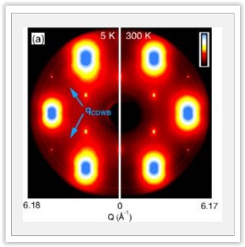
Researchers at the U.S. Department of Energy's (DOE) Ames Laboratory have discovered an unusual property of purple bronze that may point to new ways to achieve high temperature superconductivity.
While studying purple bronze, a molybdenum oxide, researchers discovered an unconventional charge density wave on its surface.
A charge density wave (CDW) is a state of matter where electrons bunch together in a repeating pattern, like a standing wave of surface of water. Superconductivity and charge density waves share a common origin, often co-exist, and can compete for dominance in certain materials.
Conventional CDWs and superconductivity both arise from electron-phonon interactions, the interaction of electrons with the vibrations of the crystal lattice. Electron-electron interactions are the likely origin of unconventional, high-temperature superconductivity such as found in copper- and iron-based compounds.
Unconventional, electron-electron driven CDW are extremely rare and its discovery here is important, because the material showed an 'extraordinary' increase of CDW transition temperature from 130K (-143°C) to 220K (-53 °C) and a huge increase of energy gap at the surface.
Both are properties essential for CDW and high-temperature superconductivity, explained Adam Kaminski, Ames Laboratory scientist and professor in the Department of Physics and Astronomy at Iowa State University.
"This was an accidental but very exciting discovery," said Kaminski. "We were studying this material because its one-dimensional structure makes it quite interesting. We saw strange things happening to the electronic band structure, but when we looked at the surface we were stunned by extraordinary enhancement of transition temperature and energy gap."
Share on:


Testimonial
"Advertising in PCB007 Magazine has been a great way to showcase our bare board testers to the right audience. The I-Connect007 team makes the process smooth and professional. We’re proud to be featured in such a trusted publication."
Klaus Koziol - atgSuggested Items
Electrodeposited Copper Foils Market to Grow by $11.7 Billion Over 2025-2032
09/18/2025 | Globe NewswireThe global electrodeposited copper foils market is poised for dynamic growth, driven by the rising adoption in advanced electronics and renewable energy storage solutions.
MacDermid Alpha Showcases Advanced Interconnect Solutions at PCIM Asia 2025
09/18/2025 | MacDermid Alpha Electronics SolutionsMacDermid Alpha Electronic Solutions, a global leader in materials for power electronics and semiconductor assembly, will showcase its latest interconnect innovations in electronic interconnect materials at PCIM Asia 2025, held from September 24 to 26 at the Shanghai New International Expo Centre, Booth N5-E30
Trouble in Your Tank: Implementing Direct Metallization in Advanced Substrate Packaging
09/15/2025 | Michael Carano -- Column: Trouble in Your TankDirect metallization systems based on conductive graphite are gaining popularity throughout the world. The environmental and productivity gains achievable with this process are outstanding. Direct metallization reduces the costs of compliance, waste treatment, and legal issues related to chemical exposure. A graphite-based direct plate system has been devised to address these needs.
Closing the Loop on PCB Etching Waste
09/09/2025 | Shawn Stone, IECAs the PCB industry continues its push toward greener, more cost-efficient operations, Sigma Engineering’s Mecer System offers a comprehensive solution to two of the industry’s most persistent pain points: etchant consumption and rinse water waste. Designed as a modular, fully automated platform, the Mecer System regenerates spent copper etchants—both alkaline and acidic—and simultaneously recycles rinse water, transforming a traditionally linear chemical process into a closed-loop system.
Driving Innovation: Depth Routing Processes—Achieving Unparalleled Precision in Complex PCBs
09/08/2025 | Kurt Palmer -- Column: Driving InnovationIn PCB manufacturing, the demand for increasingly complex and miniaturized designs continually pushes the boundaries of traditional fabrication methods, including depth routing. Success in these applications demands not only on robust machinery but also sophisticated control functions. PCB manufacturers rely on advanced machine features and process methodologies to meet their precise depth routing goals. Here, I’ll explore some crucial functions that empower manufacturers to master complex depth routing challenges.