Controlling Anisotropy
July 25, 2016 | A*STAREstimated reading time: 2 minutes

The huge energy consumption of the world’s data centers creates an urgent need to develop electronic devices that can process information with reduced power requirements. A device that harnesses the ‘spin’ of electrons offers a route toward this. A*STAR researchers show how the performance of these so-called spintronic memories can be optimized by careful control of its structure.
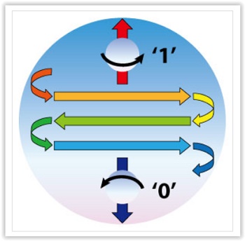
A spin-transfer torque magnetic random-access memory (STT-MRAM) comprises a stack of thin magnetic layers. One of these layers makes all the electrons in a current flowing through it have the same spin. This spin-polarized current can then change the magnetic properties of a second layer. This relies on the tendency of the electron spins in the material to align along one direction much more than it does another — a property called magnetic anisotropy.
“By having a high anisotropy, the magnet is stable and the memory is able to retain information,” explains Sze Ter Lim from the A*STAR Data Storage Institute. “However, it also means that it is more difficult to switch to the opposite direction because of an effect called damping.” Previous attempts to increase the anisotropy have also led to a proportional increase in damping.
Lim and his co-workers have now developed a STT-MRAM architecture in which the anisotropy can be increased without changing the damping. Their device has a central layer of tantalum. On either side of the central layer is a film of cobalt iron boron (CoFeB), which makes up the required magnetic layers. This in turn is sandwiched between magnesium oxide. The device is grown on a substrate and capped with another layer of tantalum.
Instead of altering the thickness of the magnetic layers, as previous studies have done, the researchers investigated the influence of the outer magnesium oxide. They showed that the anisotropy rises when the top layer thickness is increased from 1.3 nanometers to 2.5 nanometers. But the effect of this change on the damping is minimal.
Lim’s team however does not believe that this change in anisotropy is directly related to the thickness of the magnesium oxide; indeed, similar changes to the thickness of the bottom magnesium oxide film had no effect. Instead, they suggest that the top tantalum atoms intermixed with the magnesium oxide during deposition, and this degrades the interface between the magnesium oxide and the CoFeB.
“The next step is to integrate these optimized materials structures into practical devices and to evaluate its performance,” says Lim.
Testimonial
"We’re proud to call I-Connect007 a trusted partner. Their innovative approach and industry insight made our podcast collaboration a success by connecting us with the right audience and delivering real results."
Julia McCaffrey - NCAB GroupSuggested Items
Beyond Design: Slaying Signal Integrity Villains
09/17/2025 | Barry Olney -- Column: Beyond DesignHigh-speed PCB design is a balancing act, where subtle oversights can develop into major signal integrity nightmares. Some culprits lie dormant during early validation, only to reveal themselves later through workflow disruptions and elusive performance bottlenecks. Take crosstalk, for example. What begins as a stray signal coupling between traces can ripple through the design, ultimately destabilizing the power distribution network. Each of these troublemakers operates with signature tactics, but they also have well-known vulnerabilities.
Driving Innovation: Depth Routing Processes—Achieving Unparalleled Precision in Complex PCBs
09/08/2025 | Kurt Palmer -- Column: Driving InnovationIn PCB manufacturing, the demand for increasingly complex and miniaturized designs continually pushes the boundaries of traditional fabrication methods, including depth routing. Success in these applications demands not only on robust machinery but also sophisticated control functions. PCB manufacturers rely on advanced machine features and process methodologies to meet their precise depth routing goals. Here, I’ll explore some crucial functions that empower manufacturers to master complex depth routing challenges.
Global PCB Connections: Understanding the General Fabrication Process—A Designer’s Hidden Advantage
08/14/2025 | Markus Voeltz -- Column: Global PCB ConnectionsDesigners don’t need to become fabricators, but understanding the basics of PCB fabrication can save you time, money, and frustration. The more you understand what’s happening on the shop floor, the better you’ll be able to prevent downstream issues. As you move into more advanced designs like HDI, flex circuits, stacked vias, and embedded components, this foundational knowledge becomes even more critical. Remember: the fabricator is your partner.
I-Connect007 Editor’s Choice: Five Must-Reads for the Week
08/08/2025 | Andy Shaughnessy, I-Connect007If you’ve been watching the news lately, you might be tempted to opine, “What’s going on here?” In this week’s must-reads, we have a wrap-up of the latest news about U.S. tariffs with Asia, and columnist Tom Yang explains why some PCB fabrication business should remain in China. We also have a piece that examines the unprecedented growth that green manufacturing is expected to see over the next four years.
Driving Innovation: Inner Layer Alignment Methods in PCB Production
08/06/2025 | Kurt Palmer -- Column: Driving InnovationIn PCB manufacturing, precision is a fundamental requirement. Among many complex processes, the accurate registration of inner layers before lamination is one of the most critical. Much like a child's game where rings must be perfectly stacked onto a single pin, PCB manufacturers align multiple conductive and insulating layers to form a cohesive, functional board. This alignment directly affects PCB precision; tighter layer alignment results in smaller "annular rings," superior performance, and higher yields.