


 Dan’s Biz Bookshelf: Four Important Books You Need to Read (Not Just Say You Have)
 The Marketing Minute: Cracking the Code of Technical Marketing


Ultra-flat Circuits Will Have Unique Properties
July 26, 2016 | Rice UniversityEstimated reading time: 3 minutes
The old rules don’t necessarily apply when building electronic components out of two-dimensional materials, according to scientists at Rice University.
The Rice lab of theoretical physicist Boris Yakobson analyzed hybrids that put 2-D materials like graphene and boron nitride side by side to see what happens at the border. They found that the electronic characteristics of such “co-planar” hybrids differ from bulkier components.
Shrinking electronics means shrinking their components. Academic labs and industries are studying how materials like graphene may enable the ultimate in thin devices by building all the necessary circuits into an atom-thick layer.
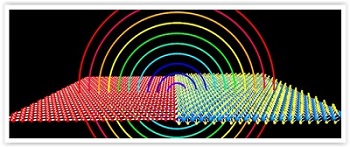
Hybrids of two-dimensional materials like the graphene-molybdenum disulfide illustrated here have electronic properties that don’t follow the same rules as their 3-D cousins, according to Rice University researchers. The limited direct contact between the two materials creates an electric field that greatly increases the size of the p/n junction. Illustration by Henry Yu
“Our work is important because semiconductor junctions are a big field,” Yakobson said. “There are books with iconic models of electronic behavior that are extremely well-developed and have become the established pillars of industry.
“But these are all for bulk-to-bulk interfaces between three-dimensional metals,” he said. “Now that people are actively working to make two-dimensional devices, especially with co-planar electronics, we realized that the rules have to be reconsidered. Many of the established models utilized in industry just don’t apply.”
The researchers led by Rice graduate student Henry Yu built computer simulations that analyze charge transfer between atom-thick materials.
“It was a logical step to test our theory on both metals and semiconductors, which have very different electronic properties,” Yu said. “This makes graphene, which is a metal — or a semimetal, to be precise — molybdenum disulfide and boron nitride, which are semiconductors, or even their hybrids ideal systems to study.
“In fact, these materials have been widely fabricated and used in the community for almost a decade, which makes analysis of them more appreciable in the field. Furthermore, both hybrids of graphene-molybdenum disulfide and graphene-boron nitride have been successfully synthesized recently, which means our study has practical meaning and can be tested in the lab now,” he said.
Yakobson said 3-D materials have a narrow region for charge transfer at the positive and negative (or p/n) junction. But the researchers found that 2-D interfaces created “a highly nonlocalized charge transfer” — and an electric field along with it — that greatly increased the junction size. That could give them an advantage in photovoltaic applications like solar cells, the researchers said.
The lab built a simulation of a hybrid of graphene and molybdenum disulfide and also considered graphene-boron nitride and graphene in which half was doped to create a p/n junction. Their calculations predicted the presence of an electric field should make 2-D Schottky (one-way) devices like transistors and diodes more tunable based on the size of the device itself.
How the atoms line up with each other is also important, Yakobson said. Graphene and boron nitride both feature hexagonal lattices, so they mesh perfectly. But molybdenum disulfide, another promising material, isn’t exactly flat, though it’s still considered 2-D.
“If the atomic structures don’t match, you get dangling bonds or defects along the borderline,” he said. “The structure has consequences for electronic behavior, especially for what is called Fermi level pinning.”
Pinning can degrade electrical performance by creating an energy barrier at the interface, Yakobson explained. “But your Schottky barrier (in which current moves in only one direction) doesn’t change as expected. This is a well-known phenomenon for semiconductors; it’s just that in two dimensions, it’s different, and in this case may favor 2-D over 3-D systems.”
Yakobson said the principles put forth by the new paper will apply to patterned hybrids of two or more 2-D patches. “You can make something special, but the basic effects are always at the interfaces. If you want to have many transistors in the same plane, it’s fine, but you still have to consider effects at the junctions.
“There’s no reason we can’t build 2-D rectifiers, transistors or memory elements,” he said. “They’ll be the same as we use routinely in devices now. But unless we develop a proper fundamental knowledge of the physics, they may fail to do what we design or plan.”
Rice postdoctoral research associate Alex Kutana is a co-author of the paper. Yakobson is the Karl F. Hasselmann Professor of Materials Science and NanoEngineering and a professor of chemistry.
The Office of Naval Research supported the research.
Share on:


Testimonial
"In a year when every marketing dollar mattered, I chose to keep I-Connect007 in our 2025 plan. Their commitment to high-quality, insightful content aligns with Koh Young’s values and helps readers navigate a changing industry. "
Brent Fischthal - Koh YoungSuggested Items
Curing and Verification in PCB Shadow Areas
09/17/2025 | Doug Katze, DymaxDesign engineers know a simple truth that often complicates electronics manufacturing: Light doesn’t go around corners. In densely populated PCBs, adhesives and coatings often fail to fully cure in shadowed regions created by tall ICs, connectors, relays, and tight housings.
Marcy’s Musings: Advancing the Advanced Materials Discussion
09/17/2025 | Marcy LaRont -- Column: Marcy's MusingsAs the industry’s most trusted global source of original content about the electronics supply chain, we continually ask you about your concerns, what you care about, and what you most want to learn about. Your responses are insightful and valuable. Thank you for caring enough to provide useful feedback and engage in dialogue.
September 2025 PCB007 Magazine: The Future of Advanced Materials
09/16/2025 | I-Connect007 Editorial TeamMoore’s Law is no more, and the advanced material solutions being developed to grapple with this reality are surprising, stunning, and perhaps a bit daunting. Buckle up for a dive into advanced materials and a glimpse into the next chapters of electronics manufacturing.
I-Connect007 Launches Advanced Electronics Packaging Digest
09/15/2025 | I-Connect007I-Connect007 is pleased to announce the launch of Advanced Electronics Packaging Digest (AEPD), a new monthly digital newsletter dedicated to one of the most critical and rapidly evolving areas of electronics manufacturing: advanced packaging at the interconnect level.
Panasonic Industry will Double the Production Capacity of MEGTRON Multi-layer Circuit Board Materials Over the Next Five Years
09/15/2025 | Panasonic Industry Co., Ltd.Panasonic Industry Co., Ltd., a Panasonic Group company, announced plans for a major expansion of its global production capacity for MEGTRON multi-layer circuit board materials today. The company plans to double its production over the next five years to meet growing demand in the AI server and ICT infrastructure markets.