


 Dan’s Biz Bookshelf: Four Important Books You Need to Read (Not Just Say You Have)
 The Marketing Minute: Cracking the Code of Technical Marketing


Watering Solar Cells Makes Them Grow… in Power!
July 27, 2016 | OISTEstimated reading time: 3 minutes
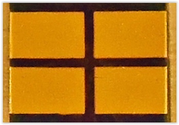
Perovskite solar cells are the rising star in the photovoltaic landscape. Since their invention, less than ten years ago, their efficiency has doubled twice and it is now over 22% – an astonishing result in the renewable energy sector. Taking the name ‘perovskite’ from the light-harvesting layer that characterizes them, these solar cells are lighter, cheaper, and more flexible than the traditional crystalline silicon-based cells.
Perovskite solar cells are usually exposed to ambient air for several hours after fabrication. This procedure increases their efficiency, even if the reason behind the phenomenon was unclear. The scientific explanation of this practice has now been discovered by researchers from the Energy Materials and Surface Sciences Unit (EMSS) at the Okinawa Institute of Science and Technology Graduate University (OIST) led by Prof Yabing Qi. Their results are published in Advanced Materials Interfaces.
“It’s intriguing: why do we need ambient air to enhance the effectiveness of perovskite solar cells?” Zafer Hawash, first author of the study and an OIST PhD student, commented. “Which component of the ambient air is linked to this phenomenon?” Starting from these questions, the researchers focused their attention on the top layer of the solar cells.
The choice was logical, because even if perovskite solar cell contains several layers – all of which may play a role in the cell efficiency – the top-most layer is the one in direct contact with ambient air. Thus, that is the layer most likely affected by the external environment. The layer is called ‘hole transport layer’, and it has a dopant, which is a substance that enhances the electrical conductivity of the material. “It is known that the dopant of the hole transport layer plays a key role in perovskite solar cells’ performance,” Hawash said. “But it was not clear how.”
The scientists performed controlled exposure of the hole transport layer to environmental gasses, focusing on oxygen, nitrogen, and moisture – water that is in a gas state. Then, they checked the electrical properties of the hole transport layer, using a variety of methods, to see if and how the inside of the transport layer changed. “What we found is that oxygen and nitrogen do not have any role in the redistribution of the dopants,” Hawash explained. “But in the case of moisture, the solar cells’ efficiency increases. This is the discovery: moisture is the air component that causes the redistribution of the dopant across the material, and thus the enhancement of the electric properties of the solar cells.”
The scientists explain this phenomenon with the structure of the transport layer, which has many pinholes that allow the passage of gasses between the ambient and the underneath material. The dopant in the transport layer is a salt – Lithium TFSI. Being a salt, the dopant has a hygroscopic nature: it absorbs water. When the solar cells are exposed to moisture, the water absorbed by the transport layer causes the dopant to redistribute. However, long time exposure to moisture has a detrimental effect on the solar cells.
During their experiments, the researchers were also able to document the role of oxygen in the solar cells’ performance. “Oxygen enhances the electrical conductivity of the transport layer as well, but this effect does not last long,” Hawash commented. “But with the right amount of exposure to moisture, the electric proprieties are irreversibly enhanced.”
Exposing the device to moisture after fabrication is then the most effective way to enhance the solar cells’ performance. Counterintuitively, then, water is what you need to have a perovskite solar cell that works properly. This finding is of high importance for the perovskite solar cells’ future, as it finally explains a common practice whose effectiveness was mostly anecdotic, and thus could now lead the way to further improvement in the perovskite solar cells’ performance.
Share on:


Testimonial
"The I-Connect007 team is outstanding—kind, responsive, and a true marketing partner. Their design team created fresh, eye-catching ads, and their editorial support polished our content to let our brand shine. Thank you all! "
Sweeney Ng - CEE PCBSuggested Items
Beyond Design: Slaying Signal Integrity Villains
09/17/2025 | Barry Olney -- Column: Beyond DesignHigh-speed PCB design is a balancing act, where subtle oversights can develop into major signal integrity nightmares. Some culprits lie dormant during early validation, only to reveal themselves later through workflow disruptions and elusive performance bottlenecks. Take crosstalk, for example. What begins as a stray signal coupling between traces can ripple through the design, ultimately destabilizing the power distribution network. Each of these troublemakers operates with signature tactics, but they also have well-known vulnerabilities.
Driving Innovation: Depth Routing Processes—Achieving Unparalleled Precision in Complex PCBs
09/08/2025 | Kurt Palmer -- Column: Driving InnovationIn PCB manufacturing, the demand for increasingly complex and miniaturized designs continually pushes the boundaries of traditional fabrication methods, including depth routing. Success in these applications demands not only on robust machinery but also sophisticated control functions. PCB manufacturers rely on advanced machine features and process methodologies to meet their precise depth routing goals. Here, I’ll explore some crucial functions that empower manufacturers to master complex depth routing challenges.
Global PCB Connections: Understanding the General Fabrication Process—A Designer’s Hidden Advantage
08/14/2025 | Markus Voeltz -- Column: Global PCB ConnectionsDesigners don’t need to become fabricators, but understanding the basics of PCB fabrication can save you time, money, and frustration. The more you understand what’s happening on the shop floor, the better you’ll be able to prevent downstream issues. As you move into more advanced designs like HDI, flex circuits, stacked vias, and embedded components, this foundational knowledge becomes even more critical. Remember: the fabricator is your partner.
I-Connect007 Editor’s Choice: Five Must-Reads for the Week
08/08/2025 | Andy Shaughnessy, I-Connect007If you’ve been watching the news lately, you might be tempted to opine, “What’s going on here?” In this week’s must-reads, we have a wrap-up of the latest news about U.S. tariffs with Asia, and columnist Tom Yang explains why some PCB fabrication business should remain in China. We also have a piece that examines the unprecedented growth that green manufacturing is expected to see over the next four years.
Driving Innovation: Inner Layer Alignment Methods in PCB Production
08/06/2025 | Kurt Palmer -- Column: Driving InnovationIn PCB manufacturing, precision is a fundamental requirement. Among many complex processes, the accurate registration of inner layers before lamination is one of the most critical. Much like a child's game where rings must be perfectly stacked onto a single pin, PCB manufacturers align multiple conductive and insulating layers to form a cohesive, functional board. This alignment directly affects PCB precision; tighter layer alignment results in smaller "annular rings," superior performance, and higher yields.