


 Dan’s Biz Bookshelf: Four Important Books You Need to Read (Not Just Say You Have)
 The Marketing Minute: Cracking the Code of Technical Marketing


Chemical Etching Method Helps Transistors Stand Tall
July 28, 2016 | University of IllinoisEstimated reading time: 3 minutes
Smaller and faster has been the trend for electronic devices since the inception of the computer chip, but flat transistors have gotten about as small as physically possible. For researchers pushing for even faster speeds and higher performance, the only way to go is up.
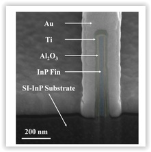
University of Illinois researchers have developed a way to etch very tall, narrow finFETs, a type of transistor that forms a tall semiconductor “fin” for the current to travel over. The etching technique addresses many problems in trying to create 3-D devices, typically done now by stacking layers or carving out structures from a thicker semiconductor wafer.
“We are exploring the electronic device roadmap beyond silicon,” said Xiuling Li, a U. of I. professor of electrical and computer engineering and the leader of the study. “With this technology, we are pushing the limit of the vertical space, so we can put more transistors on a chip and get faster speeds. We are making the structures very tall and smooth, with aspect ratios that are impossible for other existing methods to reach, and using a material with better performance than silicon.”
Typically, finFETs are made by bombarding a semiconductor wafer with beams of high-energy ions. This technique has a number of challenges, Li said. For one, the sides of the fins are sloped instead of straight up and down, making them look more like tiny mountain ranges than fins. This shape means that only the tops of the fins can perform reliably. But an even bigger problem for high-performance applications is how the ion beam damages the surface of the semiconductor, which can lead to current leakage.
The Illinois technique, called metal-assisted chemical etching or MacEtch, is a liquid-based method, which is simpler and lower-cost than using ion beams, Li said. A metal template is applied to the surface, then a chemical bath etches away the areas around the template, leaving the sides of the fins vertical and smooth.
“We use a MacEtch technique that gives a much higher aspect ratio, and the sidewalls are nearly 90 degrees, so we can use the whole volume as the conducting channel,” said graduate student Yi Song, the first author of the paper. “One very tall fin channel can achieve the same conduction as several short fin channels, so we save a lot of area by improving the aspect ratio.”
The smoothness of the sides is important, since the semiconductor fins must be overlaid with insulators and metals that touch the tiny wires that interconnect the transistors on a chip. To have consistently high performance, the interface between the semiconductor and the insulator needs to be smooth and even, Song said.
Right now, the researchers use the compound semiconductor indium phosphide with gold as the metal template. However, they are working to develop a MacEtch method that does not use gold, which is incompatible with silicon.
“Compound semiconductors are the future beyond silicon, but silicon is still the industry standard. So it is important to make it compatible with silicon and existing manufacturing processes,” Li said.
The researchers said the MacEtch technique could apply to many types of devices or applications that use 3-D semiconductor structures, such as computing memory, batteries, solar cells and LEDs.
The National Science Foundation, the International Institute for Carbon-Neutral Energy Research (I2CNER) and Lam Research supported this work. The co-authors of this work include U. of I. postdoctoral researcher Parsian Mohensi (now a professor at the Rochester Institute of Technology) and graduate student Seung Hyun Kim; Jae Cheol Shin, a professor at Yeungnam University in South Korea; Tatumi Ishihara, a professor at I2CNER in Japan; and Ilesanmi Adesida, a U. of I. professor of electrical and computer engineering. Li also is affiliated with the Micro and Nanotechnology Laboratory at the U. of I.
Share on:


Testimonial
"Advertising in PCB007 Magazine has been a great way to showcase our bare board testers to the right audience. The I-Connect007 team makes the process smooth and professional. We’re proud to be featured in such a trusted publication."
Klaus Koziol - atgSuggested Items
Indium President and CEO to Deliver ELCINA CEO Forum Keynote at Productronica India
09/17/2025 | Indium CorporationIndium Corporation President and CEO Ross Berntson will deliver the Electronic Industries Association of India (ELCINA) CEO Forum keynote at Productronica India, to be held September 17-19 in Bengaluru, India.
Indium to Highlight Energy-Efficient, High-Reliability Solder Solutions for EV and Electronics at Productronica India
09/03/2025 | Indium CorporationIndium Corporation, a leading materials refiner, smelter, manufacturer, and supplier to the global electronics, semiconductor, electric vehicle (EV), thin-film, and thermal management markets, will feature a range of sustainable, high-reliability solder products at Productronica India, to be held September 17-19 in Bengaluru, India.
Indium Promotes Huang to Senior Manager, Marketing Communications
08/28/2025 | Indium CorporationWith its commitment to innovation and growth through employee development, Indium Corporation announces the promotion of Jingya Huang to Senior Manager, Marketing Communications, to continue to lead the company’s branding and promotional efforts.
Indium Expert to Present on AI Thermal Challenges at INEMI Forum on Complex Integrated Electronics
08/26/2025 | Indium CorporationIndium Corporation Assistant Product Manager Foo Siang Hooi will deliver a technical presentation on addressing thermal challenges in AI and high-performance computing (HPC) with metal-based thermal interface materials (TIMs) at the International Electronics Manufacturing Initiative (INEMI) Forum on Complex Integrated Electronics, to be held September 17-18 in Penang, Malaysia.
Indium Corporation to Showcase Innovative Materials Enabling AI Technology at SEMICON Taiwan
08/20/2025 | Indium CorporationIndium Corporation®, a leading materials refiner, smelter, manufacturer, and supplier to the global electronics, semiconductor, AI, thin-film, and thermal management markets, will showcase its heterogeneous integration and assembly (HIA) products and thermal interface materials (TIMs) at SEMICON Taiwan, to be held September 10-12 in Taipei, Taiwan.