


 Dan’s Biz Bookshelf: Four Important Books You Need to Read (Not Just Say You Have)
 The Marketing Minute: Cracking the Code of Technical Marketing


Discovery Could Lead to New Materials for Ultra-small Components
August 2, 2016 | Department of Energy, Office of ScienceEstimated reading time: 1 minute
As any good carpenter knows, it’s often easier to get what you want if you build it yourself. An international team using resources at the Center for Functional Nanomaterials took that idea to heart. They wanted to tailor extremely small wires that carry light and electrons. They devised an approach that lets them tailor the wires through exquisite control over the structures at the nanoscale. New structures could open up a potential path to a wide range of smaller, lighter, or more efficient devices.
This development could lead to highly tailored nanowires for new classes of high-performance, energy-efficient computing, communications, and environmental and medical sensing systems. The resulting devices could lead to smaller electronics as well as improving solar panels, photodetectors, and semiconductor lasers.
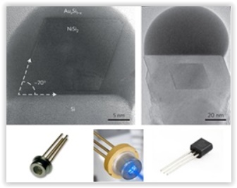
Semiconducting nanowires have a wide range of existing and potential applications in optoelectronic materials, from single-electron transistors and tunnel diodes, to light-emitting semiconducting nanowires to energy-harvesting devices. An international collaboration led by the University of Cambridge and IBM has demonstrated a new method to create novel nanowires that contain nanocrystals embedded within them. They accomplished this by modifying the classic “vapor-liquid-solid” crystal growth method, wherein a liquid-phase catalyst decomposes an incoming gas-phase source and mediates the deposition of the solid, growing nanowire. In this work, a bimetallic catalyst is used. The team showed that by appropriate thermal treatment, it is possible to crystallize a solid silicide structure within the liquid catalyst, and then attach the nanowire to the solid silicon in a controlled epitaxial fashion. The Center for Functional Nanomaterials’ Electron Microscopy Facility was employed to image the nanomaterials by high spatial-resolution, aberration-corrected transmission electron microscopy. As well, scientists used a first-of-its-kind direct electron detector to obtain high temporal-resolution images of the fabrication process. Incorporating these instruments with the expertise and insight of the scientific team led to fantastic, nanoscale control over these structures and presents notable potential for a broad range of potential devices, like photodetectors and single electron transistors.
Share on:


Testimonial
"Our marketing partnership with I-Connect007 is already delivering. Just a day after our press release went live, we received a direct inquiry about our updated products!"
Rachael Temple - AlltematedSuggested Items
Weaning the U.S. Military Off a Tablet Supply Chain That Leads to China
09/08/2025 | Jim Will, USPAETablet computers are essential to how our military fights, moves and sustains, but these devices are built on a fragile global supply chain with strong ties to China. Building domestic manufacturing to eliminate this vulnerability is feasible if we tap into the information and capabilities that already exist and create strong demand for tablets produced by trusted and assured sources.
Fresh PCB Concepts: Designing for Success at the Rigid-flex Transition Area
08/28/2025 | Team NCAB -- Column: Fresh PCB ConceptsRigid-flex PCBs come in all shapes and sizes. Manufacturers typically use fire-retardant, grade 4 (FR-4) materials in the rigid section and flexible polyimide materials in the flex region. Because of the small size, some rigid-flex PCBs, like those for hearing aid devices, are among the most challenging to manufacture. However, regardless of its size, we should not neglect the transition area between the rigid and flexible material.
Semiconductors Get Magnetic Boost with New Method from UCLA Researchers
07/31/2025 | UCLA NewsroomA new method for combining magnetic elements with semiconductors — which are vital materials for computers and other electronic devices — was unveiled by a research team led by the California NanoSystems Institute at UCLA.
Japan’s OHISAMA Project Aims to Beam Solar Power from Space This Year
07/14/2025 | I-Connect007 Editorial TeamJapan could be on the cusp of making history with its OHISAMA project in its quest to become the first country to transmit solar power from space to Earth, The Volt reported.
The Big Picture: Our Big ‘Why’ in the Age of AI
06/25/2025 | Mehul Davé -- Column: The Big PictureWith advanced technology, Tesla, Google, Microsoft, and OpenAI can quickly transform life as we know it. Several notable artificial intelligence (AI) studies, including the 2024 McKinsey Global Survey on AI, have offered insights into AI’s adoption, impact, and trajectory. The McKinsey study revealed that AI adoption continues to grow, with 50% of respondents reporting using AI in at least one business area.