


 Dan’s Biz Bookshelf: Four Important Books You Need to Read (Not Just Say You Have)
 The Marketing Minute: Cracking the Code of Technical Marketing


Ultracompact Photodetector
August 3, 2016 | KITEstimated reading time: 3 minutes
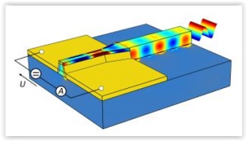
Data traffic is growing worldwide. Glass-fiber cables transmit information over long distances at the speed of light. Once they have reached their destination, however, these optical signals have to be converted into electrical signals for subsequent processing in the computer. KIT researchers have now developed a novel type of photodetector that needs far less space than conventional ones. The component has a base area of less than one millionth of a square millimeter without the data transmission rate being affected adversely. The corresponding article is published in the Optica journal.
The newly developed photodetectors, the smallest photodetectors worldwide for optical data transmission, can be used for integrated optical circuits that significantly enhance the performance of optical communication systems. Due to the small space needed, many detectors can be assembled on optical chips. In experiments, the researchers reached a data rate of up to 40 gigabits per second. “This component can transmit the contents of a complete DVD within a fraction of a second,” physicist Sascha Mühlbrandt of KIT explains. He conducted his studies at the Institute of Microstructure Technology and the Institute of Photonics and Quantum Electronics of KIT. This rate can be even further increased. “It is the so far smallest detector reaching this data rate. It is one hundred times smaller than a conventional photodetector,” Mühlbrandt emphasizes. The high-speed photodetector, called PIPED (Plasmonic Internal Photoemission Detector), is now presented by Mühlbrandt as first author, together with colleagues of KIT and ETH Zurich, in the Optica journal under the heading “Silicon-Plasmonic Internal-Photoemission Detector for 40 Gbit/s Data Reception.”
A special advantage of the reduced size is that the photodetector can be integrated with electronic components on the same CMOS chip. “Introduction of novel plasmonic components for high-speed transmission of information between electronic chips in the computer combines the advantages of electronic and optical components, while the transmission rate is comparable or even improved,” says project coordinator Professor Manfred Kohl of KIT’s Institute of Microstructure Technology. The photodetector was developed under the NAVOLCHI (Nano Scale Disruptive Silicon-Plasmonic Platform for Chip-to-Chip Interconnection) project. Under the 7th EU Research Framework Programme, the KIT project of three years’ duration in the area of information and communication technologies was funded with about EUR 500,000.
The high-performance photodetector uses so-called surface plasmon polaritons, highly concentrated electromagnetic waves at metallic-dielectric interfaces, to combine optics and electronics on smallest space. “This new class of plasmonic transceivers is based on the mechanism generating photocurrent, i.e. direct signal conversion at metallic interfaces with optical frequencies. This process is known as internal photoemission,” Mühlbrandt says. For enhancing the efficiency of light absorption and light conversion into electrical signals, charge carriers are generated at a titanium-silicon transition and taken up at another gold-silicon transition. The high rate is due to the special detector geometry: Both metal-silicon transitions are located less than one hundred billionth of a meter apart.
The researchers consider the PIPED concept to be essential not only for future optical data transmission systems, but also for wireless data transmission. “This novel approach to detecting optical signals allows for the generation and detection of electromagnetic signals with bandwidths in the terahertz range,” says Professor Christian Koos of KIT, Spokesperson of the Helmholtz International Research School for Teratronics (HIRST) that focuses on the combination of photonic and electronic processes for ultra-rapid signal processing. “Plasmonic components might be used in wireless high-speed communication and allow for transmission rates of up to 1 terabit per second. “Research related to PIPED was also supported by the EnTeraPIC Starting Grant of the European Research Council, the Helmholtz International Research School for Teratronics (HIRST) at KIT, at which the disciplines of physics, electrical engineering, computer science, and mechanical engineering cooperate, as well as by KIT’s “Karlsruhe Nano-Micro Facility” (KNMF) platform.
Share on:


Testimonial
"In a year when every marketing dollar mattered, I chose to keep I-Connect007 in our 2025 plan. Their commitment to high-quality, insightful content aligns with Koh Young’s values and helps readers navigate a changing industry. "
Brent Fischthal - Koh YoungSuggested Items
Soaring Inference AI Demand Triggers Severe Nearline HDD Shortages; QLC SSD Shipments Poised for Breakout in 2026
09/16/2025 | TrendForceTrendForce’s latest investigations reveal that the massive data volumes generated by AI are straining the global infrastructure of data center storage.
Advanced Packaging-to-Board-Level Integration: Needs and Challenges
09/15/2025 | Devan Iyer and Matt Kelly, Global Electronics AssociationHPC data center markets now demand components with the highest processing and communication rates (low latencies and high bandwidth, often both simultaneously) and highest capacities with extreme requirements for advanced packaging solutions at both the component level and system level. Insatiable demands have been projected for heterogeneous compute, memory, storage, and data communications. Interconnect has become one of the most important pillars of compute for these systems.
Procense Raises $1.5M in Seed Funding to Accelerate AI-Powered Manufacturing
09/11/2025 | BUSINESS WIREProcense, a San Francisco-based industrial automation startup developing cutting-edge AI and remote sensing technologies for process manufacturers has raised $1.5 million in a seed funding round led by Kevin Mahaffey, Business Insider’s #1 seed investor of 2025 and HighSage Ventures, a Boston-based family office that primarily invests in public and private companies in the global software, internet, consumer, and financial technology sectors.
Zuken Announces E3.series 2026 Release for Accelerated Electrical Design and Enhanced Engineering Productivity
09/10/2025 | ZukenZuken reveals details of the upcoming 2026 release of E3.series, which will introduce powerful new features aimed at streamlining electrical and fluid design, enhancing multi-disciplinary collaboration, and boosting engineering productivity.
AI Infrastructure Boosts Global Semiconductor Revenue Growth to 17.6% in 2025
09/09/2025 | IDCAccording to the Worldwide Semiconduct o r Technology and Supply Chain Intelligence service from International Data Corporation (IDC), worldwide semiconductor revenue is expected to reach $800 billion in 2025, growing 17.6% year-over-year from $680 billion in 2024. This follows a strong rebound in 2024, when revenue grew by 22.4% year-over-year.