


 Dan’s Biz Bookshelf: Four Important Books You Need to Read (Not Just Say You Have)
 The Marketing Minute: Cracking the Code of Technical Marketing


Material Can Lead to New Optical Devices
August 3, 2016 | AMERICAN INSTITUTE OF PHYSICSEstimated reading time: 3 minutes
Invisibility cloaks have less to do with magic than with metamaterials. These human-engineered materials have properties that don't occur in nature, allowing them to bend and manipulate light in weird ways. For example, some of these materials can channel light around an object so that it appears invisible at a certain wavelength. These materials are also useful in applications such as smaller, faster, and more energy efficient optics, sensors, light sources, light detectors and telecommunications devices.
Now researchers have designed a new kind of metamaterial whose properties can be changed with a flick of a switch. In their proof-of-principle experiment, the researchers used germanium antimony telluride (GST) -- the kind of phase-change material found in CDs and DVDs -- to make an improved switchable metasurface that can block or transmit particular wavelengths of light at the command of light pulses. The researchers describe the metamaterial this week in Applied Physics Letters, from AIP Publishing, and how its ability to switch properties can be used in a range of sophisticated optical devices.
"Technologies based upon the control and manipulation of light are all around us and of fundamental importance to modern society," said Kevin MacDonald, a researcher at the University of Southampton in the U.K. "Metamaterials are part of the process of finding new ways to use light and do new things with it -- they are an enabling technology platform for 21st century optics."
By dynamically controlling the optical properties of materials, you can modulate, select, or switch characteristics of light beams, such as intensity, phase, color and direction -- an ability that's essential to many existing and potential devices, he said.
Switchable metamaterials in general aren't new. MacDonald and many others have made such materials before by combining metallic metamaterials with so-called active media such as GST, which can respond to external stimuli like heat, light or an electric field. In these hybrid materials, the metal component is structurally engineered at the nanometer scale to provide the desired optical properties. Incorporating the active medium provides a way to tune or switch those properties.
The problem is that metals tend to absorb light at visible and infrared wavelengths, making them unsuitable for many optical device applications. Melting points are also suppressed in nanostructured metals, making the metamaterials susceptible to damage from laser beams. In addition, a typical metal is gold, which isn't compatible with the CMOS technology that's ubiquitous in making today's integrated devices.
In the new work, MacDonald and his colleagues at Southampton's Optoelectronics Research Centre & Centre for Photonic Metamaterials have made a switchable metamaterial that doesn't use metal at all. "What we've done now is structure the phase-change material itself," MacDonald said. "We have created what is known as an all-dielectric metamaterial, with the added benefit of GST's nonvolatile phase-switching behavior."
Pulses of laser light can change the structure of GST between a random, amorphous one and a crystalline one. For GST, this behavior is nonvolatile, which means it will stay in a particular state until another pulse switches it back. In rewritable CDs and DVDs, this binary laser-driven switching is the basis for data storage.
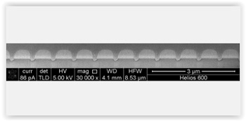
The researchers created metamaterial grating patterns in an amorphous GST film only 300 nm thick, with lines 750 to 950 nanometers apart. This line spacing allows the surfaces to selectively block the transmission of light at near-infrared wavelengths (between 1300 and 1600 nm). But when a green laser converts the surfaces into a crystalline state, they become transparent at these wavelengths.
The research team is now working to make metamaterials that can switch back and forth over many cycles. They're also planning increasingly complex structures to deliver more sophisticated optical functions. For example, this approach could be used to make switchable ultra-thin metasurface lenses and other flat, optical components.
Share on:


Testimonial
"The I-Connect007 team is outstanding—kind, responsive, and a true marketing partner. Their design team created fresh, eye-catching ads, and their editorial support polished our content to let our brand shine. Thank you all! "
Sweeney Ng - CEE PCBSuggested Items
Curing and Verification in PCB Shadow Areas
09/17/2025 | Doug Katze, DymaxDesign engineers know a simple truth that often complicates electronics manufacturing: Light doesn’t go around corners. In densely populated PCBs, adhesives and coatings often fail to fully cure in shadowed regions created by tall ICs, connectors, relays, and tight housings.
Marcy’s Musings: Advancing the Advanced Materials Discussion
09/17/2025 | Marcy LaRont -- Column: Marcy's MusingsAs the industry’s most trusted global source of original content about the electronics supply chain, we continually ask you about your concerns, what you care about, and what you most want to learn about. Your responses are insightful and valuable. Thank you for caring enough to provide useful feedback and engage in dialogue.
September 2025 PCB007 Magazine: The Future of Advanced Materials
09/16/2025 | I-Connect007 Editorial TeamMoore’s Law is no more, and the advanced material solutions being developed to grapple with this reality are surprising, stunning, and perhaps a bit daunting. Buckle up for a dive into advanced materials and a glimpse into the next chapters of electronics manufacturing.
I-Connect007 Launches Advanced Electronics Packaging Digest
09/15/2025 | I-Connect007I-Connect007 is pleased to announce the launch of Advanced Electronics Packaging Digest (AEPD), a new monthly digital newsletter dedicated to one of the most critical and rapidly evolving areas of electronics manufacturing: advanced packaging at the interconnect level.
Panasonic Industry will Double the Production Capacity of MEGTRON Multi-layer Circuit Board Materials Over the Next Five Years
09/15/2025 | Panasonic Industry Co., Ltd.Panasonic Industry Co., Ltd., a Panasonic Group company, announced plans for a major expansion of its global production capacity for MEGTRON multi-layer circuit board materials today. The company plans to double its production over the next five years to meet growing demand in the AI server and ICT infrastructure markets.