


 Dan’s Biz Bookshelf: Four Important Books You Need to Read (Not Just Say You Have)
 The Marketing Minute: Cracking the Code of Technical Marketing


Swapping Substrates Improves Edges of Graphene Nanoribbons
August 4, 2016 | AIP.orgEstimated reading time: 2 minutes
It is now feasible to make a prized material for spintronic devices and semiconductors -- monolayer graphene nanoribbons with zigzag edges.
Miniscule ribbons of graphene are highly sought-after building blocks for semiconductor devices because of their predicted electronic properties. But making these nanostructures has remained a challenge. Now, a team of researchers from China and Japan have devised a new method to make the structures in the lab. Their findings appear in the current issue of Applied Physics Letters, from AIP Publishing.
"Many studies have predicted the properties of graphene nanoribbons with zigzag edges," said Guangyu Zhang, senior author on the study. "But in experiments it's very hard to actually make this material."
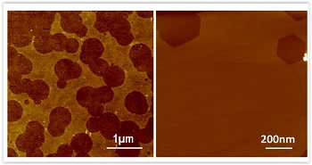
Previously, researchers have tried to make graphene nanoribbons by placing sheets of graphene over a layer of silica and using atomic hydrogen to etch strips with zigzag edges, a process known as anisotropic etching. These edges are crucial to modulate the nanoribbon's properties.
But this method only worked well to make ribbons that had two or more graphene layers. Irregularities in silica created by electronic peaks and valleys roughen its surface, so creating precise zigzag edges on graphene monolayers was a challenge. Zhang and his colleagues from the Chinese Academy of Sciences, Beijing Key Laboratory for Nanomaterials and Nanodevices, and the Collaborative Innovation Center of Quantum Matter teamed up with Japanese collaborators from the National Institute for Materials Science to solve the problem.
They replaced the underlying silica with boron nitride, a crystalline material that's chemically sluggish and has a smooth surface devoid of electronic bumps and pits. By using this substrate and the anisotropic etching technique, the group successfully made graphene nanoribbons that were only one-layer thick, and had well-defined zigzag edges.
"This is the first time we have ever seen that graphene on a boron nitride surface can be fabricated in such a controllable way," Zhang explained.
The zigzag-edged nanoribbons showed high electron mobility in the range of 2000 cm2/Vs even at widths of less than 10nm -- the highest value ever reported for these structures -- and created clean, narrow energy band gaps, which makes them promising materials for spintronic and nano-electronic devices.
"When you decrease the width of the nanoribbons, the mobility decreases drastically because of edge defects," said Zhang. "Using standard lithography fabrication techniques, studies have seen mobility of 100 cm2/Vs or even lower, but our material still exceeds 2000 cm2/Vs even at the sub-10 nanometer scale, demonstrating that these nanoribbons are of very high quality."
In future studies, extending this method to other kinds of substrates could enable the quick large scale processing of monolayers of graphene to make high-quality nanoribbons with zigzag edges.
Share on:


Testimonial
"In a year when every marketing dollar mattered, I chose to keep I-Connect007 in our 2025 plan. Their commitment to high-quality, insightful content aligns with Koh Young’s values and helps readers navigate a changing industry. "
Brent Fischthal - Koh YoungSuggested Items
Breakthrough in Non-Contact Solder Removal Earns Kurtz Ersa 2025 Mexico Technology Award at SMTA Guadalajara
09/18/2025 | Kurtz Ersa Inc.Kurtz Ersa Inc., a leading supplier of electronics production equipment, is proud to announce that it has been awarded a 2025 Mexico Technology Award in the category of Rework & Repair for its HR 600P Automatic Rework System.
A.R.T. Invests in Latest Equipment to Further Enhance Electronics Training Facilities
09/17/2025 | A.R.T. Ltd.Advanced Rework Technology Ltd. (A.R.T.), a leading independent IPC-accredited training provider, has announced a series of new equipment investments at its state-of-the-art training centre.
Richardson Electronics Appoints Daniel Albers to Drive Made-in-USA Contract Manufacturing Expansion
09/17/2025 | Globe NewswireRichardson Electronics, Ltd., a global provider of engineered solutions for the green energy, power management, and custom display markets, announced the appointment of Daniel Albers to spearhead business development for its expanded, Made-in-USA contract manufacturing efforts.
STMicroelectronics to Advance Next-generation Chip Manufacturing Technology with New PLP Pilot Line in Tours, France
09/17/2025 | STMicroelectronicsSTMicroelectronics, a global semiconductor leader serving customers across the spectrum of electronics applications, today announced new details regarding the development of the next generations of Panel-Level Packaging (PLP) technology through a pilot line in its Tours site, France, which is expected to be operational in Q3 2026.
Indium President and CEO to Deliver ELCINA CEO Forum Keynote at Productronica India
09/17/2025 | Indium CorporationIndium Corporation President and CEO Ross Berntson will deliver the Electronic Industries Association of India (ELCINA) CEO Forum keynote at Productronica India, to be held September 17-19 in Bengaluru, India.