


 Dan’s Biz Bookshelf: Four Important Books You Need to Read (Not Just Say You Have)
 The Marketing Minute: Cracking the Code of Technical Marketing


Tiny High-performance Solar Cells Turn Power Generation Sideways
August 4, 2016 | University of Wisconsin-MadisonEstimated reading time: 3 minutes
University of Wisconsin—Madison engineers have created high-performance, micro-scale solar cells that outshine comparable devices in key performance measures. The miniature solar panels could power myriad personal devices — wearable medical sensors, smartwatches, even autofocusing contact lenses.
Large, rooftop photovoltaic arrays generate electricity from charges moving vertically. The new, small cells, described today (Aug. 3, 2016) in the journal Advanced Materials Technologies, capture current from charges moving side-to-side, or laterally. And they generate significantly more energy than other sideways solar systems.
New-generation lateral solar cells promise to be the next big thing for compact devices because arranging electrodes horizontally allows engineers to sidestep a traditional solar cell fabrication process: the arduous task of perfectly aligning multiple layers of the cell’s material atop one another.
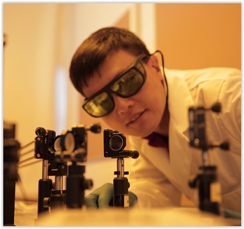
Hongrui Jiang inspects the alignment of a light source to illuminate new-generation lateral solar cells. The solar cells developed by Jiang’s group harvest almost three times more electricity from incoming light as compared to existing technologies. Photo: Stephanie Precourt
“From a fabrication point of view, it is always going to be easier to make side-by-side structures,” says Hongrui Jiang, a UW–Madison professor of electrical and computer engineering and corresponding author on the paper. “Top-down structures need to be made in multiple steps and then aligned, which is very challenging at small scales.”
Lateral solar cells also offer engineers greater flexibility in materials selection.
Top-down photovoltaic cells are made up of two electrodes surrounding a semiconducting material like slices of bread around the meat in a sandwich. When light hits the top slice, charge travels through the filling to the bottom layer and creates electric current.
In the top-down arrangement, one layer needs to do two jobs: It must let in light and transmit charge. Therefore, the material for one electrode in a typical solar cell must be not only highly transparent, but also electrically conductive. And very few substances perform both tasks well.
Instead of building its solar cell sandwich one layer at a time, Jiang’s group created a densely packed, side-by-side array of miniature electrodes on top of transparent glass. The resulting structure — akin to an entire loaf of bread’s worth of solar-cell sandwiches standing up sideways on a clear plate — separates light-harvesting and charge-conducting functions between the two components.
Generally, synthesizing such sideways sandwiches is no simple matter. Other approaches that rely on complicated internal nanowires or expensive materials called perovskites fall short on multiple measures of solar cell quality.
“We easily beat all of the other lateral structures,” says Jiang.
Existing top-of the-line lateral new-generation solar cells convert merely 1.8 percent of incoming light into useful electricity. Jiang’s group nearly tripled that measure, achieving up to 5.2 percent efficiency.
“In other structures, a lot of volume goes wasted because there are no electrodes or the electrodes are mismatched,” says Jiang. “The technology we developed allows us to make very compact lateral structures that take advantage of the full volume.”
Packing so many electrodes into such a small volume boosted the devices’ “fill factors,” a metric related to the maximum attainable power, voltage and current. The structures realized fill factors up to 0.6 — more than twice the demonstrated maximum for other lateral new-generation solar cells.
Jiang and colleagues are working to make their solar cells even smaller and more efficient by exploring materials that further optimize transparency and conductivity. Ultimately they plan to develop a small-scale, flexible solar cell that could provide power to an electrically tunable contact lens.
Other authors on the paper included Xi Zhang, Yinggang Huang, Hao Bian, Hewei Liu, and Xuezhen Huang. The National Institutes of Health provided funding for the research.
Share on:


Testimonial
"Advertising in PCB007 Magazine has been a great way to showcase our bare board testers to the right audience. The I-Connect007 team makes the process smooth and professional. We’re proud to be featured in such a trusted publication."
Klaus Koziol - atgSuggested Items
Curing and Verification in PCB Shadow Areas
09/17/2025 | Doug Katze, DymaxDesign engineers know a simple truth that often complicates electronics manufacturing: Light doesn’t go around corners. In densely populated PCBs, adhesives and coatings often fail to fully cure in shadowed regions created by tall ICs, connectors, relays, and tight housings.
Marcy’s Musings: Advancing the Advanced Materials Discussion
09/17/2025 | Marcy LaRont -- Column: Marcy's MusingsAs the industry’s most trusted global source of original content about the electronics supply chain, we continually ask you about your concerns, what you care about, and what you most want to learn about. Your responses are insightful and valuable. Thank you for caring enough to provide useful feedback and engage in dialogue.
September 2025 PCB007 Magazine: The Future of Advanced Materials
09/16/2025 | I-Connect007 Editorial TeamMoore’s Law is no more, and the advanced material solutions being developed to grapple with this reality are surprising, stunning, and perhaps a bit daunting. Buckle up for a dive into advanced materials and a glimpse into the next chapters of electronics manufacturing.
I-Connect007 Launches Advanced Electronics Packaging Digest
09/15/2025 | I-Connect007I-Connect007 is pleased to announce the launch of Advanced Electronics Packaging Digest (AEPD), a new monthly digital newsletter dedicated to one of the most critical and rapidly evolving areas of electronics manufacturing: advanced packaging at the interconnect level.
Panasonic Industry will Double the Production Capacity of MEGTRON Multi-layer Circuit Board Materials Over the Next Five Years
09/15/2025 | Panasonic Industry Co., Ltd.Panasonic Industry Co., Ltd., a Panasonic Group company, announced plans for a major expansion of its global production capacity for MEGTRON multi-layer circuit board materials today. The company plans to double its production over the next five years to meet growing demand in the AI server and ICT infrastructure markets.