


 Dan’s Biz Bookshelf: ‘Elevate: Push Beyond Your Limits'
 The Marketing Minute: The First Step to More Sales—Marketing
 It’s Only Common Sense: Customer Service Is Sales in Disguise


Heraeus and Intego Show a New Optical Inspection Method for Patterned Touch Sensors
August 4, 2016 | HeraeusEstimated reading time: 2 minutes
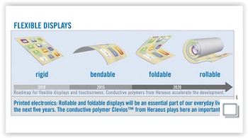
At this year Touch Taiwan from August 24-26, Heraeus launches a new touch panel process to pattern Clevios conductive polymer films by DFR (dry-film resist) photolithography. It enables high resolution patterns required for advanced touch sensor designs of flexible smartphones and tablets. Heraeus worked together with Intego on a new inspection method to visualize the invisible patterns of the Clevios sensor films. “With Intego, we found an excellent partner to offer a solution that enables our customers to accelerate the adoption of Clevios touch technology in mass production for flexible touch displays”, says Dr. Armin Sautter, Head of Technical Service Display at Heraeus. High resolution patterning of touch sensors is a prerequisite for advanced touch panels, especially for flexible and foldable touch displays. Dr. Thomas Wagner, CEO at Intego GmbH, emphazises “This is an important milestone, we are now able to offer a customized tool and a process for the inspection and quality control of the sensor patterning process for production environment.” A small scale demo tool will be shown at the Heraeus booth Taipei World Trade Center / Nangang Exhibition Hall 4F / N1029.
Patterned ITO films require additional optical compensation layers to hide the visible patterns in the touch panel. In contrast, both fine and wide Clevios patterns are already completely invisible after touch sensor production. No additional optical compensation layers are required in the touch panel process, offering customers cost benefits as well as process simplifications. Clevios conductive polymers are key materials for foldable touch sensors that will be used in the coming generations of flexible smartphones and tablets. Clevios coated films can be folded more than 300.000 times at a radius as low as 1 mm without degradation of the electro-optical properties.
About Intego GmbH
Intego GmbH, located in Erlangen, Germany, develops inspection systems for automated production lines used in a number of industries including glass/sapphire, solar, LED/OLED, electronics, automotive, plastics and medical technologies. (www.intego.de/en)
About Heraeus
Heraeus, the technology group headquartered in Hanau, Germany, is a leading international family-owned company formed in 1851. With expertise, a focus on innovations, operational excellence and an entrepreneurial leadership, we strive to continuously improve our business performance. We create high-quality solutions for our clients and strengthen their competitiveness in the long term by combining material expertise with technological know-how. Our ideas are focused on themes such as the environment, energy, health, mobility and industrial applications. Our portfolio ranges from components to coordinated material systems which are used in a wide variety of industries, including the steel, electronics, chemical, automotive and telecommunications industries. In the 2015 financial year, Heraeus generated revenues without precious metals of €1.9 bn and a total revenue of €12.9 bn. With approximately 12,500 employees worldwide in more than 100 subsidiaries in 38 countries, Heraeus holds a leading position in its global markets.
Share on:


Suggested Items
Knocking Down the Bone Pile: Addressing End-of-life Component Solderability Issues, Part 4
07/16/2025 | Nash Bell -- Column: Knocking Down the Bone PileIn 1983, the Department of Defense identified that over 40% of military electronic system failures in the field were electrical, with approximately 50% attributed to poor solder connections. Investigations revealed that plated finishes, typically nickel or tin, were porous and non-intermetallic.
Digital Twin Concept in Copper Electroplating Process Performance
07/11/2025 | Aga Franczak, Robrecht Belis, Elsyca N.V.PCB manufacturing involves transforming a design into a physical board while meeting specific requirements. Understanding these design specifications is crucial, as they directly impact the PCB's fabrication process, performance, and yield rate. One key design specification is copper thieving—the addition of “dummy” pads across the surface that are plated along with the features designed on the outer layers. The purpose of the process is to provide a uniform distribution of copper across the outer layers to make the plating current density and plating in the holes more uniform.
The Knowledge Base: A Conference for Cleaning and Coating of Mission-critical Electronics
07/08/2025 | Mike Konrad -- Column: The Knowledge BaseIn electronics manufacturing, there’s a dangerous misconception that cleaning and coating are standalone options, that they operate in different lanes, and that one can compensate for the other. Let’s clear that up now. Cleaning and conformal coating are not separate decisions. They are two chapters in the same story—the story of reliability.
SMT007 Magazine July—What’s Your Competitive Sweet Spot?
07/01/2025 | I-Connect007 Editorial TeamAre you in a niche that’s growing or shrinking? Is it time to reassess and refocus? We spotlight companies thriving by redefining or reinforcing their niche—what are their insights? In the July 2025 issue of SMT007 Magazine, we spotlight companies thriving by redefining or reinforcing their niche and offer insights to help you evaluate your own.
Smarter Machines Use AOI to Transform PCB Inspections
06/30/2025 | Marcy LaRont, PCB007 MagazineAs automated optical inspection (AOI) evolves from traditional end-of-process inspections to proactive, in-line solutions, the integration of AI and machine learning is revolutionizing defect reduction and enhancing yields, marking a pivotal shift in how quality is managed in manufacturing.