


 Dan’s Biz Bookshelf: Four Important Books You Need to Read (Not Just Say You Have)
 The Marketing Minute: Cracking the Code of Technical Marketing


Two Become One: How to Turn Green Light Blue
August 11, 2016 | KITEstimated reading time: 2 minutes
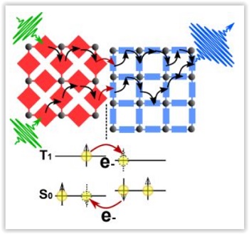
The upconversion of photons allows for a more efficient use of light: Two photons are converted into a single photon having higher energy. Researchers at KIT now showed for the first time that the inner interfaces between surface-mounted metal-organic frameworks (SURMOFs) are suited perfectly for this purpose – they turned green light blue. The result, which is now being published in the Advanced Materials journal, opens up new opportunities for optoelectronic applications such as solar cells or LEDs.
Metal-organic frameworks (MOFs) are highly ordered molecular systems that consist of metallic clusters and organic ligands. At the Institute of Functional Interfaces (IFG) of KIT, researchers developed MOFs that grow epitaxially on the surfaces of substrates. These SURMOFs (surface-mounted metal-organic frameworks) can be produced from various materials and be customized using different pore sizes and chemical functionalities so that they are suited for a broad range of applications, e.g. for sensors, catalysts, diaphragms, in medical device technology or as intelligent storage elements.
Another field of application is optoelectronics, i.e. components that are capable of converting light into electrical energy or vice versa. Many of these components work on the basis of semiconductors. “The SURMOFs combine the advantages of organic and anorganic semiconductors,” Professor Christof Wöll, Director of IFG, explains. “They feature chemical diversity and crystallinity, allowing us to create ordered heterostructures.” In many optoelectronic components, a so-called heterojunction – this is an interfacing layer between two different semiconductor materials – controls the energy transfer between the various excited states. Researches of the KIT Institute of Microstructure Technology (IMT) now created a new piggyback SURMOF in which a second SURMOF grew epitaxially, i.e. layer by layer, on a first one. At this heterojunction, it was possible to achieve photon upconversion, transforming two low-energy photons into a single photon with higher energy, by virtually fusing them together. “This process turns green light blue. Blue light has a shorter wavelength and yields more energy. This is very important for photovoltaics applications,” explains Professor Bryce Richards, Director of IMT. The scientists are presenting their work in Advanced Materials, one of the leading journals for materials science.
The photon upconversion process shown by the Karlsruhe researchers is based on the so-called triplet-triplet annihilation. Two molecules are involved: a sensitizer molecule that absorbs photons and creates triplet excited states, and an emitter molecule that takes over the triplet excited states and, by using triplet-triplet annihilation, sends out a photon that yields a higher energy than the photons that were originally absorbed. “The challenge was to create this process as efficiently as possible,” explains Dr. Ian Howard, leader of a junior research group at IMT. “We matched the sensitizer and emitter layers in a way to obtain a low conversion threshold and a higher light efficiency at the same time.”
Since the triplet transfer is based on the exchange of electrons, the photon upconversion process revealed by the researchers includes an electron transfer across the interface between the two SURMOFs. This suggests the assumption that SURMOF-SURMOF heterojunctions are suitable for many optoelectronic applications such as LEDs and solar cells. One of the limitations for the efficiency of today’s solar cells is due to the fact that they can only use photons with a certain minimum energy for electric power generation. By using upconversion, photovoltaic systems could become much more efficient.
Share on:


Testimonial
"We’re proud to call I-Connect007 a trusted partner. Their innovative approach and industry insight made our podcast collaboration a success by connecting us with the right audience and delivering real results."
Julia McCaffrey - NCAB GroupSuggested Items
Curing and Verification in PCB Shadow Areas
09/17/2025 | Doug Katze, DymaxDesign engineers know a simple truth that often complicates electronics manufacturing: Light doesn’t go around corners. In densely populated PCBs, adhesives and coatings often fail to fully cure in shadowed regions created by tall ICs, connectors, relays, and tight housings.
Marcy’s Musings: Advancing the Advanced Materials Discussion
09/17/2025 | Marcy LaRont -- Column: Marcy's MusingsAs the industry’s most trusted global source of original content about the electronics supply chain, we continually ask you about your concerns, what you care about, and what you most want to learn about. Your responses are insightful and valuable. Thank you for caring enough to provide useful feedback and engage in dialogue.
September 2025 PCB007 Magazine: The Future of Advanced Materials
09/16/2025 | I-Connect007 Editorial TeamMoore’s Law is no more, and the advanced material solutions being developed to grapple with this reality are surprising, stunning, and perhaps a bit daunting. Buckle up for a dive into advanced materials and a glimpse into the next chapters of electronics manufacturing.
I-Connect007 Launches Advanced Electronics Packaging Digest
09/15/2025 | I-Connect007I-Connect007 is pleased to announce the launch of Advanced Electronics Packaging Digest (AEPD), a new monthly digital newsletter dedicated to one of the most critical and rapidly evolving areas of electronics manufacturing: advanced packaging at the interconnect level.
Panasonic Industry will Double the Production Capacity of MEGTRON Multi-layer Circuit Board Materials Over the Next Five Years
09/15/2025 | Panasonic Industry Co., Ltd.Panasonic Industry Co., Ltd., a Panasonic Group company, announced plans for a major expansion of its global production capacity for MEGTRON multi-layer circuit board materials today. The company plans to double its production over the next five years to meet growing demand in the AI server and ICT infrastructure markets.