


 Dan’s Biz Bookshelf: Four Important Books You Need to Read (Not Just Say You Have)
 The Marketing Minute: Cracking the Code of Technical Marketing


Quantum Dots with Impermeable Shell: A Powerful Tool for Nanoengineering
August 11, 2016 | Institute of Physical Chemistry of the Polish Academy of SciencesEstimated reading time: 4 minutes
Unique optical features of quantum dots make them an attractive tool for many applications, from cutting-edge displays to medical imaging. Physical, chemical or biological properties of quantum dots must, however, be adapted to the desired needs. Unfortunately, up to now quantum dots prepared by chemical methods could be functionalized using copper-based click reactions with retention of their luminescence. This obstacle can be ascribed to the fact that copper ions destroy the ability of quantum dots to emit light. Scientists from the Institute of Physical Chemistry of the Polish Academy of Sciences (IPC PAS) in Warsaw and the Faculty of Chemistry of the Warsaw University of Technology (FC WUT) have shown, however, that zinc oxide (ZnO) quantum dots prepared by an original method developed by them, after modification by the click reaction with the participation of copper ions, fully retain their ability to emit light.
"Click reactions catalyzed by copper cations have long attracted the attention of chemists dealing with quantum dots. The experimental results, however, were disappointing: after modification, the luminescence was so poor that they were just not fit for use. We were the first to demonstrate that it is possible to produce quantum dots from organometallic precursors in a way they do not lose their valuable optical properties after being subjected to copper-catalysed click reactions," says Prof. Janusz Lewinski (IPC PAS, FC WUT).
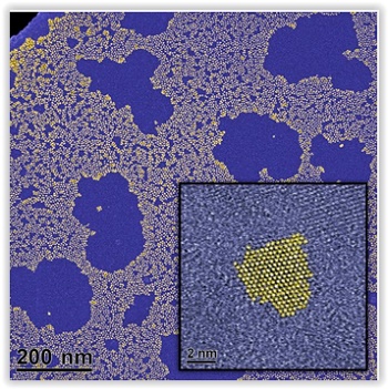
Quantum dots are crystalline structures with size of a few nanometers (billionth parts of a meter). As semiconductor materials, they exhibit a variety of interesting features typical of quantum objects, including absorbing and emitting radiation of only a strictly defined energy. Since atoms interact with light in a similar way, quantum dots are often called artificial atoms. In some respects, however, quantum dots offer more possibilities than atoms. Optical properties of each dot actually depend on its size and the type of material from which it is formed. This means that quantum dots may be precisely designed for specific applications.
To meet the need of specific applications, quantum dots have to be tailored in terms of physico-chemical properties. For this purpose, chemical molecules with suitable characteristics are attached to their surface. Due to the simplicity, efficacy, and speed of the process, an exceptionally convenient method is the click reaction. Unfortunately, one of the most widely used click reactions takes place with the participation of copper ions, which was reported to result in the almost complete quenching of the luminescence of the quantum dots.
"Failure is usually a result of the inadequate quality of quantum dots, which is determined by the synthesis method. Currently, ZnO dots are mainly produced by the sol-gel method from inorganic precursors. Quantum dots generated in this manner are coated with a heterogeneous and probably leaky protective shell, made of various sorts of chemical molecules. During a click reaction, the copper ions are in direct contact with the surface of quantum dots and quench the luminescence of the dot, which becomes completely useless," explains Dr. Agnieszka Grala (IPC PAS), the first author of the article in the Chemical Communications journal.
For several years, Prof. Lewinski's team has been developing alternative methods for the preparation of high quality ZnO quantum dots. The method presented in this paper affords the quantum dots derived from organozinc precursors. Composition of the nanoparticles can be programmed at the stage of precursors preparation, which makes it possible to precisely control the character of their organic-inorganic interface.
"Nanoparticles produced by our method are crystalline and all have almost the same size. They are spherical and have characteristics of typical quantum dots. Every nanoparticle is stabilized by an impermeable protective jacket, built of organic compounds, strongly anchored on the surface of the semiconductor core. As a result, our quantum dots remain stable for a long time and do not aggregate, that is clump together, in solutions," describes Malgorzata Wolska-Pietkiewicz, a PhD student at FC WUT.
"The key to success is producing a uniform stabilizing shell. Such coatings are characteristic of the ZnO quantum dots obtained by our method. The organic layer behaves as a tight protective umbrella protecting dots from direct influence of the copper ions," says Dr. Grala and clarifies: "We carried out click reaction known as alkyne-azide cycloaddition, in which we used a copper(l) compound as catalysts. After functionalization, our quantum dots shone as brightly as at the beginning."
Quantum dots keep finding more and more applications in various industrial processes and as nanomarkers in, among others, biology and medicine, where they are combined with biologically active molecules. Nanoobjects functionalized in this manner are used to label both individual cells as well as whole tissues. The unique properties of quantum dots also enable long-term monitoring of the labelled item. Commonly used quantum dots, however, contain toxic heavy metals, including cadmium. In addition, they clump together in solutions, which supports the thesis of the lack of tightness of their shells. Meanwhile, the ZnO dots produced by Prof. Lewinski's group are non-toxic, they do not aggregate, and can be bound to many chemical compounds - so they are much more suitable for medical diagnosis and for imaging cells and tissues.
Share on:


Testimonial
"In a year when every marketing dollar mattered, I chose to keep I-Connect007 in our 2025 plan. Their commitment to high-quality, insightful content aligns with Koh Young’s values and helps readers navigate a changing industry. "
Brent Fischthal - Koh YoungSuggested Items
Trouble in Your Tank: Implementing Direct Metallization in Advanced Substrate Packaging
09/15/2025 | Michael Carano -- Column: Trouble in Your TankDirect metallization systems based on conductive graphite are gaining popularity throughout the world. The environmental and productivity gains achievable with this process are outstanding. Direct metallization reduces the costs of compliance, waste treatment, and legal issues related to chemical exposure. A graphite-based direct plate system has been devised to address these needs.
Closing the Loop on PCB Etching Waste
09/09/2025 | Shawn Stone, IECAs the PCB industry continues its push toward greener, more cost-efficient operations, Sigma Engineering’s Mecer System offers a comprehensive solution to two of the industry’s most persistent pain points: etchant consumption and rinse water waste. Designed as a modular, fully automated platform, the Mecer System regenerates spent copper etchants—both alkaline and acidic—and simultaneously recycles rinse water, transforming a traditionally linear chemical process into a closed-loop system.
Driving Innovation: Depth Routing Processes—Achieving Unparalleled Precision in Complex PCBs
09/08/2025 | Kurt Palmer -- Column: Driving InnovationIn PCB manufacturing, the demand for increasingly complex and miniaturized designs continually pushes the boundaries of traditional fabrication methods, including depth routing. Success in these applications demands not only on robust machinery but also sophisticated control functions. PCB manufacturers rely on advanced machine features and process methodologies to meet their precise depth routing goals. Here, I’ll explore some crucial functions that empower manufacturers to master complex depth routing challenges.
Trouble in Your Tank: Minimizing Small-via Defects for High-reliability PCBs
08/27/2025 | Michael Carano -- Column: Trouble in Your TankTo quote the comedian Stephen Wright, “If at first you don’t succeed, then skydiving is not for you.” That can be the battle cry when you find that only small-diameter vias are exhibiting voids. Why are small holes more prone to voids than larger vias when processed through electroless copper? There are several reasons.
The Government Circuit: Navigating New Trade Headwinds and New Partnerships
08/25/2025 | Chris Mitchell -- Column: The Government CircuitAs global trade winds continue to howl, the electronics manufacturing industry finds itself at a critical juncture. After months of warnings, the U.S. Government has implemented a broad array of tariff increases, with fresh duties hitting copper-based products, semiconductors, and imports from many nations. On the positive side, tentative trade agreements with Europe, China, Japan, and other nations are providing at least some clarity and counterbalance.