


 Dan’s Biz Bookshelf: Four Important Books You Need to Read (Not Just Say You Have)
 The Marketing Minute: Cracking the Code of Technical Marketing


Nanomaterial Safety Screening Could Become Faster, Cheaper with New Laboratory Test
August 15, 2016 | UCLAEstimated reading time: 2 minutes
UCLA researchers have designed a laboratory test that uses microchip technology to predict how potentially hazardous nanomaterials could be.
According to UCLA professor Huan Meng, certain engineered nanomaterials, such as non-purified carbon nanotubes that are used to strengthen commercial products, could have the potential to injure the lungs if inhaled during the manufacturing process. The new test he helped develop could be used to analyze the extent of the potential hazard.
The same test could also be used to identify biological biomarkers that can help scientists and doctors detect cancer and infectious diseases. Currently, scientists identify those biomarkers using other tests; one of the most common is called enzyme-linked immunosorbent assay, or ELISA. But the new platform, which is called semiconductor electronic label-free assay, or SELFA, costs less and is faster and more accurate, according to research published in the journal Scientific Reports.
The study was led by Meng, a UCLA assistant adjunct professor of medicine, and Chi On Chui, a UCLA associate professor of electrical engineering and bioengineering.
ELISA has been used by scientists for decades to analyze biological samples — for example, to detect whether epithelial cells in the lungs that have been exposed to nanomaterials are inflamed. But ELISA must be performed in a laboratory setting by skilled technicians, and a single test can cost roughly $700 and take five to seven days to process.
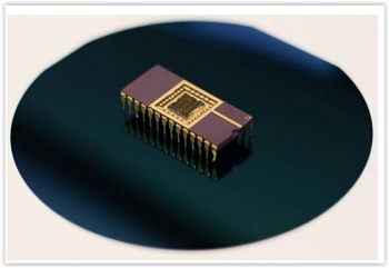
In contrast, SELFA uses microchip technology to analyze samples. The test can take between 30 minutes and two hours and, according to the UCLA researchers, could cost just a few dollars per sample when high-volume production begins.
The SELFA chip contains a T-shaped nanowire that acts as an integrated sensor and amplifier. To analyze a sample, scientists place it on a sensor on the chip. The vertical part of the T-shaped nanowire converts the current from the molecule being analyzed, and the horizontal portion amplifies that signal to distinguish the molecule from others.
The use of the T-shaped nanowires created in Chui’s lab is a new application of a UCLA patented invention that was developed by Chui and his colleagues. The device is the first time that “lab-on-a-chip” analysis has been tested in a scenario that mimics a real-life situation.
The UCLA scientists exposed cultured lung cells to different nanomaterials and then compared their results using SELFA with results in a database of previous studies that used other testing methods.
“By measuring biomarker concentrations in the cell culture, we showed that SELFA was 100 times more sensitive than ELISA,” Meng said. “This means that not only can SELFA analyze much smaller sample sizes, but also that it can minimize false-positive test results.”
Chui said, “The results are significant because SELFA measurement allows us to predict the inflammatory potential of a range of nanomaterials inside cells and validate the prediction with cellular imaging and experiments in animals’ lungs.”
Other authors were UCLA graduate student Yufei Mao, UCLA postdoctoral scholar Kyeong-Sik Shin, and UCLA staff scientists Xiang Wang and Zhaoxia Ji.
The research was supported by the National Science Foundation, the Environmental Protection Agency and the University of California Center for Environmental Implications of Nanotechnology.
Share on:


Testimonial
"In a year when every marketing dollar mattered, I chose to keep I-Connect007 in our 2025 plan. Their commitment to high-quality, insightful content aligns with Koh Young’s values and helps readers navigate a changing industry. "
Brent Fischthal - Koh YoungSuggested Items
TTCI and The Training Connection Strengthen Electronics Manufacturing with Test Services and Training at PCB West 2025
09/16/2025 | The Test Connection Inc.The Test Connection Inc. (TTCI), a trusted provider of electronic test and manufacturing solutions, and The Training Connection LLC (TTC-LLC) will exhibit at PCB West 2025, taking place Wednesday, October 1, 2025, at the Santa Clara Convention Center in California. Visitors are invited to Booth 113 to explore the companies’ complementary expertise in test engineering services and workforce development for the electronics industry.
Smart Eye Receives Milestone AIS Order from Fleet Safety Company Optix
09/11/2025 | Smart EyeSmart Eye, a global leader in Human Insight AI and Driver Monitoring Systems (DMS), announced a milestone order for its AIS system from Optix, a global provider of fleet management solutions. Initially, in 2025, 4,000 commercial vehicles will be equipped with Smart Eye’s technology, marking the first wave of deployments globally.
Datest Unveils Viscom iX7059 XL 3D CT AXI System
08/25/2025 | DatestDatest, a trusted leader in advanced testing, engineering, inspection, and failure analysis services, and the go-to destination for when your boards misbehave and your AXI line goes on vacation, is thrilled to announce the arrival of its newest diagnostic weapon: the Viscom iX7059 XL 3D CT AXI Inspection System.
Gardien Services Installs Customized G93 Flying Probe Tester – Largest Test Area in North America/Europe
09/07/2025 | Gardien GroupGardien Group is proud to announce the successful installation of a customized G93 Flying Probe Test Machine at a major manufacturer in North America. This cutting-edge system features the largest test area of any flying probe tester in North America and Europe, setting a new benchmark for PCB testing capabilities.
Meet with The Test Connection Inc. (TTCI) at SMTA Guadalajara 2025
08/18/2025 | The Test Connection Inc.The Test Connection Inc. (TTCI), a trusted provider of electronic test and manufacturing solutions for more than 45 years, is pleased to announce its participation at the upcoming SMTA Guadalajara Expo & Tech Forum, taking place September 17–18, 2025, at Expo Guadalajara, Salón Jalisco Hall D & E.