


 Dan’s Biz Bookshelf: Four Important Books You Need to Read (Not Just Say You Have)
 The Marketing Minute: Cracking the Code of Technical Marketing


Booting up Spin-based Device Studies
August 16, 2016 | MITEstimated reading time: 3 minutes
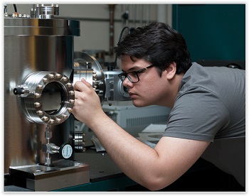
MIT Materials Processing Center (MPC)-Center for Materials Science and Engineering (CMSE) Summer Scholar Grant Smith is working in the lab of MIT assistant professor of electrical engineering and computer science Luqiao Liu, to create special thin film materials suitable for spin-based devices such as magnetic tunnel junctions used in computer memory.
For his summer project, Smith is operating a sputter deposition chamber, where he grows ultrathin films from 2 to 10 nanometers thick. He is making devices that are precursors to a memory device and measuring their properties.
Magnetic tunnel junctions used in spin-based systems for computer memory got their start with a key breakthrough in 1994 at MIT by research scientist Jagadeesh S. Moodera and colleagues. They are especially valued because they retain information even when the power is off.
A magnetic tunnel junction pairs two thin film materials, each with a special property called ferromagnetism. “Those ferromagnetic layers can either have their magnetizations aligned or anti-aligned,” Smith explains. If they are aligned, that is their magnetic fields both point in the same direction, the electrons in one layer will have more states available for them in the other layer, but if they are anti-aligned [with magnetic fields pointing in opposite directions], there will be fewer states for electrons available in that other layer.
Change in Resistance
“When you’re trying to push a current through and the magnetizations are aligned, the resistance is much lower. So if you fix one of the magnetic layers and flip the other one based on whether you want it to be a zero or a one or if you’re just trying to detect the existence of a magnetic field, you’ll be able to see something on the order of a 100 to 300 percent change in the resistance of that device,” Smith says. This is about 10 to 30 times greater that the approximately 10 percent shift in resistance in the first such devices.
Smith is working with a dual-layer of an antiferromagnet called iridium manganese and a ferromagnet called cobalt iron boron. “Those two in conjunction, when you condition them in a specific way, they pin the magnetization of the one ferromagnet in that one specific direction. So that is your fixed layer,” he explains.
For his summer project, Smith seeks to establish that ability to grow these magnetic tunnel junctions in Liu’s lab, and if that is a success, to try to manipulate that magnetization with the spin texture of a topological semimetal in order to do switching.
Nice spot to be
“I’m just happy to learn anything about this field basically,” says Smith, a rising senior at Penn State University majoring in physics, who hopes to pursue a doctorate in the sciences. “I’m glad to be learning how to manufacture these magnetic tunnel junctions. That’s a really important skill. They’re used everywhere as far as doing experiments in this field. They’re useful in industry. It’s actually a very nice spot to be in.”
Liu, who joined the MIT faculty in September 2015, says, “So far I have been very glad with Grant Smith's performance. Having a summer intern working in our lab does provide a good advantage to our research as it allows us to look into directions that we were not able to previously due to a shortage of manpower. Moreover, Mr. Smith is really diligent and smart. It is a very nice experience so far to work with such a motivated undergraduate student.”
For Smith, working in Liu’s lab on materials at room temperature is a change of pace from his work at Penn State on materials at extremely low temperatures in the range of 4 kelvins (-452.47 degrees Fahrenheit). “When you’re working with these sort of things you can learn about new behaviors, new scientific phenomenon,” he says. “Here everything is very room temperature focused working much closer towards, working much more closely with the place industry is at right now,” Smith says.
Share on:


Testimonial
"In a year when every marketing dollar mattered, I chose to keep I-Connect007 in our 2025 plan. Their commitment to high-quality, insightful content aligns with Koh Young’s values and helps readers navigate a changing industry. "
Brent Fischthal - Koh YoungSuggested Items
Curing and Verification in PCB Shadow Areas
09/17/2025 | Doug Katze, DymaxDesign engineers know a simple truth that often complicates electronics manufacturing: Light doesn’t go around corners. In densely populated PCBs, adhesives and coatings often fail to fully cure in shadowed regions created by tall ICs, connectors, relays, and tight housings.
Marcy’s Musings: Advancing the Advanced Materials Discussion
09/17/2025 | Marcy LaRont -- Column: Marcy's MusingsAs the industry’s most trusted global source of original content about the electronics supply chain, we continually ask you about your concerns, what you care about, and what you most want to learn about. Your responses are insightful and valuable. Thank you for caring enough to provide useful feedback and engage in dialogue.
September 2025 PCB007 Magazine: The Future of Advanced Materials
09/16/2025 | I-Connect007 Editorial TeamMoore’s Law is no more, and the advanced material solutions being developed to grapple with this reality are surprising, stunning, and perhaps a bit daunting. Buckle up for a dive into advanced materials and a glimpse into the next chapters of electronics manufacturing.
I-Connect007 Launches Advanced Electronics Packaging Digest
09/15/2025 | I-Connect007I-Connect007 is pleased to announce the launch of Advanced Electronics Packaging Digest (AEPD), a new monthly digital newsletter dedicated to one of the most critical and rapidly evolving areas of electronics manufacturing: advanced packaging at the interconnect level.
Panasonic Industry will Double the Production Capacity of MEGTRON Multi-layer Circuit Board Materials Over the Next Five Years
09/15/2025 | Panasonic Industry Co., Ltd.Panasonic Industry Co., Ltd., a Panasonic Group company, announced plans for a major expansion of its global production capacity for MEGTRON multi-layer circuit board materials today. The company plans to double its production over the next five years to meet growing demand in the AI server and ICT infrastructure markets.