


 Dan’s Biz Bookshelf: Four Important Books You Need to Read (Not Just Say You Have)
 The Marketing Minute: Cracking the Code of Technical Marketing


Miniaturized Sensor that Can Measure Chemistry on a Chip
August 17, 2016 | Cornell UniversityEstimated reading time: 3 minutes
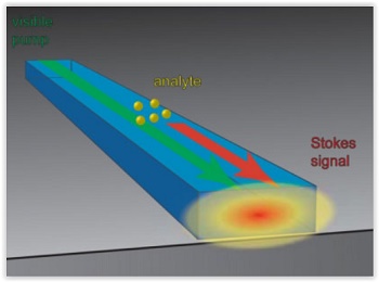
The researchers use a phenomenon called “Raman scattering,” when a laser strikes a molecule it kicks back the laser energy as photons of light at a variety of wavelengths that depend on the structure and composition of the molecule.
To allow this phenomenon to occur on a chip, researchers fire a laser into a waveguide – a strip of transparent material made of titanium dioxide, where the light bounces off the inside surfaces and becomes confined to the waveguide. Because a waveguide is only a few nanometers (billionths a meter) high, the light waves spread out beyond the waveguide, creating a so-called “evanescent field” above the surface of the chip. The pumping laser can induce Raman scattering in the space above the chip, or in a drop of liquid placed on its surface for analysis, while still confining the light wave to the chip. Light kicked back by the excited molecules also follows the waveguide; a prism at the end of the waveguide can spread that light into a spectrum that is a “fingerprint” identifying the molecule that produced it.
Nanoscale Waveguide
Light traveling through a nanoscale waveguide on a hip spreads beyond the waveguide and can interact with molecules above the surface of the chip.
“If you need a chemical sensor in the lab, that is not a problem,” said Jin Suntivich, assistant professor of materials science and engineering. “But when you are outside, finding a chemical sensor that you can take with you is a challenge. We want to develop a technology that is small enough for a phone, such that your personal electronics can constantly monitor the world around you, and the moment you see something out of the ordinary, the sensor can tell you what it is.”
Sensors based on Raman scattering have been made before, using silicon nitride waveguides. The Cornell researchers have come up with a design that could make a sensor more sensitive and small enough to be used in the field by using a new material, titanium dioxide.
“We’re not the first but we’re the best,” said Christopher Evans, a Kavli Postdoctoral Fellow in the Laboratory of Atomic and Solid State Physics and the Kavli Institute at Cornell for Nanoscale Science. Evans is first author of paper describing the new approach published in the July 14 online edition of the American Chemical Society journal ACS Photonics ("TiO2 Nanophotonic Sensors for Efficient Integrated Evanescent Raman Spectroscopy"). Co-authors are Suntivich and Chengyu Liu, a doctoral student in the School of Applied and Engineering Physics.
Circular Waveguide
A circular waveguide tangent to a straight guide causes light to circulate around and around, giving it more time to interact with material above the chip. The ring is about the diameter of a human hair.
Titanium dioxide has a much higher refractive index, making a greater contrast with the space above the chip, which creates a stronger evanescent field. The material is also transparent to light at visible wavelengths, a condition that allows researchers to use a laser at shorter, visible wavelengths, which induce better scattering. The researchers tested with a green laser pointer as a light source.
For a future device, a tiny laser unit can be built into a chip, as can a component that can spread out the wavelengths of the kicked off light onto a photosensitive device to read the spectrum. One possibility is to read the spectrum with the camera in a phone.
Interaction of the pumping laser with the material above the chip increases with the length of the waveguide. But the researchers also offer a way to increase the interaction without having to make the chip larger. The solution is a “ring resonator.” When a circular waveguide is set tangent to a straight guide, some of the light will enter the ring and continue to circle around it, letting the light interact continually with the material above the chip many times. The circumference of the ring can be adjusted to resonate with the wavelength of the light, intensifying the effect. “We have shown that we can increase the amount of peak signal from our sensors by an order of magnitude (or more), while simultaneously reducing the device footprint down to the cross-section of a human hair,” Evans said.
Potential applications include portable sensors to monitor air and water quality or conduct laboratory tests in the field. Chemists could and observe chemical reactions while they occur.
Share on:


Testimonial
"Our marketing partnership with I-Connect007 is already delivering. Just a day after our press release went live, we received a direct inquiry about our updated products!"
Rachael Temple - AlltematedSuggested Items
Curing and Verification in PCB Shadow Areas
09/17/2025 | Doug Katze, DymaxDesign engineers know a simple truth that often complicates electronics manufacturing: Light doesn’t go around corners. In densely populated PCBs, adhesives and coatings often fail to fully cure in shadowed regions created by tall ICs, connectors, relays, and tight housings.
Marcy’s Musings: Advancing the Advanced Materials Discussion
09/17/2025 | Marcy LaRont -- Column: Marcy's MusingsAs the industry’s most trusted global source of original content about the electronics supply chain, we continually ask you about your concerns, what you care about, and what you most want to learn about. Your responses are insightful and valuable. Thank you for caring enough to provide useful feedback and engage in dialogue.
September 2025 PCB007 Magazine: The Future of Advanced Materials
09/16/2025 | I-Connect007 Editorial TeamMoore’s Law is no more, and the advanced material solutions being developed to grapple with this reality are surprising, stunning, and perhaps a bit daunting. Buckle up for a dive into advanced materials and a glimpse into the next chapters of electronics manufacturing.
I-Connect007 Launches Advanced Electronics Packaging Digest
09/15/2025 | I-Connect007I-Connect007 is pleased to announce the launch of Advanced Electronics Packaging Digest (AEPD), a new monthly digital newsletter dedicated to one of the most critical and rapidly evolving areas of electronics manufacturing: advanced packaging at the interconnect level.
Panasonic Industry will Double the Production Capacity of MEGTRON Multi-layer Circuit Board Materials Over the Next Five Years
09/15/2025 | Panasonic Industry Co., Ltd.Panasonic Industry Co., Ltd., a Panasonic Group company, announced plans for a major expansion of its global production capacity for MEGTRON multi-layer circuit board materials today. The company plans to double its production over the next five years to meet growing demand in the AI server and ICT infrastructure markets.