


 Dan’s Biz Bookshelf: Four Important Books You Need to Read (Not Just Say You Have)
 The Marketing Minute: Cracking the Code of Technical Marketing


Scientists Uncover the Origin of High-Temperature Superconductivity in Copper-Oxide Compound
August 18, 2016 | BNLEstimated reading time: 4 minutes
Since the 1986 discovery of high-temperature superconductivity in copper-oxide compounds called cuprates, scientists have been trying to understand how these materials can conduct electricity without resistance at temperatures hundreds of degrees above the ultra-chilled temperatures required by conventional superconductors. Finding the mechanism behind this exotic behavior may pave the way for engineering materials that become superconducting at room temperature. Such a capability could enable lossless power grids, more affordable magnetically levitated transit systems, and powerful supercomputers, and change the way energy is produced, transmitted, and used globally.
Now, physicists at the U.S. Department of Energy's (DOE) Brookhaven National Laboratory have an explanation for why the temperature at which cuprates become superconducting is so high. After growing and analyzing thousands of samples of a cuprate known as LSCO for the four elements it contains (lanthanum, strontium, copper, and oxygen), they determined that this "critical" temperature is controlled by the density of electron pairs—the number of electron pairs per unit area. This finding, described in a Nature paper published August 17, challenges the standard theory of superconductivity, which proposes that the critical temperature depends instead on the strength of the electron pairing interaction.
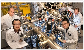
"Solving the enigma of high-temperature superconductivity has been the focus of condensed matter physics for more than 30 years," said Ivan Bozovic, a senior physicist in Brookhaven Lab's Condensed Matter Physics and Materials Science Department who led the study. "Our experimental finding provides a basis for explaining the origin of high-temperature superconductivity in the cuprates—a basis that calls for an entirely new theoretical framework."
Our experimental finding provides a basis for explaining the origin of high-temperature superconductivity in the cuprates—a basis that calls for an entirely new theoretical framework.
According to Bozovic, one of the reasons cuprates have been so difficult to study is because of the precise engineering required to generate perfect crystallographic samples that contain only the high-temperature superconducting phase.
"It is a materials science problem. Cuprates can have up to 50 atoms per unit cell and the elements can form hundreds of different compounds, likely resulting in a mixture of different phases," said Bozovic.
That's why Bozovic and his research team grew their more than 2,500 LSCO samples by using a custom-designed molecular beam epitaxy system that places single atoms onto a substrate, layer by layer. This system is equipped with advanced surface-science tools, such as those for absorption spectroscopy and electron diffraction, that provide real-time information about the surface morphology, thickness, chemical composition, and crystal structure of the resulting thin films.
"Monitoring these characteristics ensures there aren't any irregular geometries, defects, or precipitates from secondary phases in our samples," Bozovic explained.
In engineering the LSCO films, Bozovic chemically added strontium atoms, which produce mobile electrons that pair up in the copper-oxide layers where superconductivity occurs. This "doping" process allows LSCO and other cuprates—normally insulating materials—to become superconducting.
For this study, Bozovic added strontium in amounts beyond the doping level required to induce superconductivity. Earlier studies on this "overdoping" had indicated that the density of electron pairs decreases as the doping concentration is increased. Scientists had tried to explain this surprising experimental finding by attributing it to different electronic orders competing with superconductivity, or electron pair breaking caused by impurities or disorder in the lattice. For example, they had thought that geometrical defects, such as displaced or missing atoms, could be at play.
Brookhaven Lab physicist Ivan Bozovic explains why a copper-oxide compound can conduct electricity without resistance at temperatures well above those required by conventional superconductors.
To test these explanations, Bozovic and his team measured the magnetic and electronic properties of their engineered LSCO films. They used a technique called mutual inductance to determine the magnetic penetration depth (the distance a magnetic field transmits through a superconductor), which indicates the density of electron pairs.
Their measurements established a precise linear relationship between the critical temperature and electron pair density: both continue to decrease as more dopant is added, until no electrons pair up at all, while the critical temperature drops to near-zero Kelvin (minus 459 degrees Fahrenheit). According to the standard understanding of metals and conventional superconductors, this result is unexpected because LSCO becomes more metallic the more it is overdoped.
"Disorder, phase separation, or electron pair breaking would have the reverse effect by introducing scattering that impedes the flow of electrons, thus making the material more resistive, i.e., less metallic," said Bozovic.
If Bozovic's team is correct that critical temperature is controlled by electron pair density, then it seems that small, local pairs of electrons are behind the high temperature at which cuprates become superconducting. Previous experiments have established that the size of electron pairs is much smaller in cuprates than in conventional superconductors, whose pairs are so large that they overlap. Understanding what interaction makes the electron pairs so small in cuprates is the next step in the quest to solve the mystery of high-temperature superconductivity.
Bozovic's team included Brookhaven physicists Anthony Bollinger and Jie Wu, supported by funding provided by DOE's Office of Science, and postdoctoral researcher Xi He, supported by the Gordon and Betty Moore Foundation.
Share on:


Testimonial
"Our marketing partnership with I-Connect007 is already delivering. Just a day after our press release went live, we received a direct inquiry about our updated products!"
Rachael Temple - AlltematedSuggested Items
Trouble in Your Tank: Implementing Direct Metallization in Advanced Substrate Packaging
09/15/2025 | Michael Carano -- Column: Trouble in Your TankDirect metallization systems based on conductive graphite are gaining popularity throughout the world. The environmental and productivity gains achievable with this process are outstanding. Direct metallization reduces the costs of compliance, waste treatment, and legal issues related to chemical exposure. A graphite-based direct plate system has been devised to address these needs.
Closing the Loop on PCB Etching Waste
09/09/2025 | Shawn Stone, IECAs the PCB industry continues its push toward greener, more cost-efficient operations, Sigma Engineering’s Mecer System offers a comprehensive solution to two of the industry’s most persistent pain points: etchant consumption and rinse water waste. Designed as a modular, fully automated platform, the Mecer System regenerates spent copper etchants—both alkaline and acidic—and simultaneously recycles rinse water, transforming a traditionally linear chemical process into a closed-loop system.
Driving Innovation: Depth Routing Processes—Achieving Unparalleled Precision in Complex PCBs
09/08/2025 | Kurt Palmer -- Column: Driving InnovationIn PCB manufacturing, the demand for increasingly complex and miniaturized designs continually pushes the boundaries of traditional fabrication methods, including depth routing. Success in these applications demands not only on robust machinery but also sophisticated control functions. PCB manufacturers rely on advanced machine features and process methodologies to meet their precise depth routing goals. Here, I’ll explore some crucial functions that empower manufacturers to master complex depth routing challenges.
Trouble in Your Tank: Minimizing Small-via Defects for High-reliability PCBs
08/27/2025 | Michael Carano -- Column: Trouble in Your TankTo quote the comedian Stephen Wright, “If at first you don’t succeed, then skydiving is not for you.” That can be the battle cry when you find that only small-diameter vias are exhibiting voids. Why are small holes more prone to voids than larger vias when processed through electroless copper? There are several reasons.
The Government Circuit: Navigating New Trade Headwinds and New Partnerships
08/25/2025 | Chris Mitchell -- Column: The Government CircuitAs global trade winds continue to howl, the electronics manufacturing industry finds itself at a critical juncture. After months of warnings, the U.S. Government has implemented a broad array of tariff increases, with fresh duties hitting copper-based products, semiconductors, and imports from many nations. On the positive side, tentative trade agreements with Europe, China, Japan, and other nations are providing at least some clarity and counterbalance.