


 Dan’s Biz Bookshelf: Four Important Books You Need to Read (Not Just Say You Have)
 The Marketing Minute: Cracking the Code of Technical Marketing


Graphene Nanoribbons in Solutions Mimic Nature
August 22, 2016 | Rice UniversityEstimated reading time: 3 minutes
Graphene nanoribbons (GNRs) bend and twist easily in solution, making them adaptable for biological uses like DNA analysis, drug delivery and biomimetic applications, according to scientists at Rice University.
Knowing the details of how GNRs behave in a solution will help make them suitable for wide use in biomimetics, according to Rice physicist Ching-Hwa Kiang, whose lab employed its unique capabilities to probe nanoscale materials like cells and proteins in wet environments. Biomimetic materials are those that imitate the forms and properties of natural materials.
The research led by recent Rice graduate Sithara Wijeratne, now a postdoctoral researcher at Harvard University, appears in the Nature journal Scientific Reports.
Graphene nanoribbons can be thousands of times longer than they are wide. They can be produced in bulk by chemically “unzipping” carbon nanotubes, a process invented by Rice chemist and co-author James Tour and his lab.
Their size means they can operate on the scale of biological components like proteins and DNA, Kiang said. “We study the mechanical properties of all different kinds of materials, from proteins to cells, but a little different from the way other people do,” she said. “We like to see how materials behave in solution, because that’s where biological things are.” Kiang is a pioneer in developing methods to probe the energy states of proteins as they fold and unfold.
She said Tour suggested her lab have a look at the mechanical properties of GNRs. “It’s a little extra work to study these things in solution rather than dry, but that’s our specialty,” she said.
Nanoribbons are known for adding strength but not weight to solid-state composites, like bicycle frames and tennis rackets, and forming an electrically active matrix. A recent Rice project infused them into an efficient de-icer coating for aircraft.
But in a squishier environment, their ability to conform to surfaces, carry current and strengthen composites could also be valuable.
“It turns out that graphene behaves reasonably well, somewhat similar to other biological materials. But the interesting part is that it behaves differently in a solution than it does in air,” she said. The researchers found that like DNA and proteins, nanoribbons in solution naturally form folds and loops, but can also form helicoids, wrinkles and spirals.
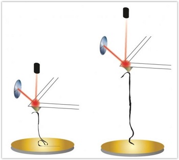
Kiang, Wijeratne and Jingqiang Li, a co-author and student in the Kiang lab, used atomic force microscopy to test their properties. Atomic force microscopy can not only gather high-resolution images but also take sensitive force measurements of nanomaterials by pulling on them. The researchers probed GNRs and their precursors, graphene oxide nanoribbons.
The researchers discovered that all nanoribbons become rigid under stress, but their rigidity increases as oxide molecules are removed to turn graphene oxide nanoribbons into GNRs. They suggested this ability to tune their rigidity should help with the design and fabrication of GNR-biomimetic interfaces.
“Graphene and graphene oxide materials can be functionalized (or modified) to integrate with various biological systems, such as DNA, protein and even cells,” Kiang said. “These have been realized in biological devices, biomolecule detection and molecular medicine. The sensitivity of graphene bio-devices can be improved by using narrow graphene materials like nanoribbons.”
Wijeratne noted graphene nanoribbons are already being tested for use in DNA sequencing, in which strands of DNA are pulled through a nanopore in an electrified material. The base components of DNA affect the electric field, which can be read to identify the bases.
The researchers saw nanoribbons’ biocompatibility as potentially useful for sensors that could travel through the body and report on what they find, not unlike the Tour lab’s nanoreporters that retrieve information from oil wells.
Further studies will focus on the effect of the nanoribbons’ width, which range from 10 to 100 nanometers, on their properties.
Co-authors are Rice research scientist Evgeni Penev; graduate student Wei Lu; alumna Amanda Duque, now a scientist at Los Alamos National Laboratory; and Boris Yakobson, the Karl F. Hasselmann Professor of Materials Science and NanoEngineering and a professor of chemistry. Tour is the T.T. and W.F. Chao Professor of Chemistry as well as a professor of computer science and of materials science and nanoengineering. Kiang is an associate professor of physics and astronomy and of bioengineering.
The Welch Foundation and the National Science Foundation supported the research. The researchers used the NSF’s Extreme Science and Engineering Discovery Environment and the NSF-supported DAVinCI supercomputer administered by Rice’s Center for Research Computing and procured in a partnership with Rice’s Ken Kennedy Institute.
Share on:


Testimonial
"We’re proud to call I-Connect007 a trusted partner. Their innovative approach and industry insight made our podcast collaboration a success by connecting us with the right audience and delivering real results."
Julia McCaffrey - NCAB GroupSuggested Items
Curing and Verification in PCB Shadow Areas
09/17/2025 | Doug Katze, DymaxDesign engineers know a simple truth that often complicates electronics manufacturing: Light doesn’t go around corners. In densely populated PCBs, adhesives and coatings often fail to fully cure in shadowed regions created by tall ICs, connectors, relays, and tight housings.
Marcy’s Musings: Advancing the Advanced Materials Discussion
09/17/2025 | Marcy LaRont -- Column: Marcy's MusingsAs the industry’s most trusted global source of original content about the electronics supply chain, we continually ask you about your concerns, what you care about, and what you most want to learn about. Your responses are insightful and valuable. Thank you for caring enough to provide useful feedback and engage in dialogue.
September 2025 PCB007 Magazine: The Future of Advanced Materials
09/16/2025 | I-Connect007 Editorial TeamMoore’s Law is no more, and the advanced material solutions being developed to grapple with this reality are surprising, stunning, and perhaps a bit daunting. Buckle up for a dive into advanced materials and a glimpse into the next chapters of electronics manufacturing.
I-Connect007 Launches Advanced Electronics Packaging Digest
09/15/2025 | I-Connect007I-Connect007 is pleased to announce the launch of Advanced Electronics Packaging Digest (AEPD), a new monthly digital newsletter dedicated to one of the most critical and rapidly evolving areas of electronics manufacturing: advanced packaging at the interconnect level.
Panasonic Industry will Double the Production Capacity of MEGTRON Multi-layer Circuit Board Materials Over the Next Five Years
09/15/2025 | Panasonic Industry Co., Ltd.Panasonic Industry Co., Ltd., a Panasonic Group company, announced plans for a major expansion of its global production capacity for MEGTRON multi-layer circuit board materials today. The company plans to double its production over the next five years to meet growing demand in the AI server and ICT infrastructure markets.