


 The Marketing Minute: Cracking the Code of Technical Marketing
 Trouble in Your Tank: Implementing Direct Metallization in Advanced Substrate Packaging


Tiny Lasers that Opens New Era for Light-based Computing
August 22, 2016 | HKUSTEstimated reading time: 1 minute
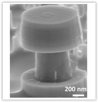
Researchers at The Hong Kong University of Science and Technology (HKUST) have fabricated microscopically-small lasers directly on silicon, enabling the future-generation microprocessors to run faster and less power-hungry – a significant step towards light-based computing.
The innovation, made by Prof Kei-may Lau, Fang Professor of Engineering and Chair Professor of the Department of Electronic and Computer Engineering, in collaboration with the University of California, Santa Barbara; Sandia National Laboratories and Harvard University, marks a major breakthrough for the semiconductor industry and well beyond.
Silicon forms the basis of everything from solar cells to the integrated circuits at the heart of our modern electronic gadgets. However, the crystal lattice of silicon and of typical laser materials could not match up, making it impossible to integrate the two materials until now, when Prof Lau’s group managed to integrate subwavelength cavities — the essential building blocks of their tiny lasers — onto silicon, allowing them to create and demonstrate high-density on-chip light-emitting elements. The finding was recently published as the cover story on Applied Physics Letters.
“These whispering gallery mode lasers are extremely attractive light source for on-chip optical communications, data processing and chemical sensing applications,” Prof Lau said. “Putting lasers on microprocessors boosts their capabilities and allows them to run at much lower powers – a big step towards photonics and electronics integration on the silicon platform and a key solution to the next-generation green information technology.”
For years, photonics had been the most energy-efficient and cost-effective method to transmit large volumes of data over long distances, now with these new silicon-based integrated lasers, photonics may be able to use for short-distance data transmission as well, which is set to greatly enhance the speed of data communication.
In fabricating these “whispering gallery mode lasers”, Prof Lau’s team etched nano-patterns directly onto the silicon, so as to confine the defects of its crystal lattices while ensuring the necessary quantum confinement of electrons within quantum dots grown on this template. Her team then use optical pumping – a process that uses light to raise or “pump” electrons from a lower energy level to a higher one, to demonstrate that the devices they created were able to operate as lasers.
These tiny lasers measure only 1 micron in diameter, and are 1,000 times shorter in length and 1 million times smaller in area than those currently used.
Share on:


Testimonial
"The I-Connect007 team is outstanding—kind, responsive, and a true marketing partner. Their design team created fresh, eye-catching ads, and their editorial support polished our content to let our brand shine. Thank you all! "
Sweeney Ng - CEE PCBSuggested Items
Curing and Verification in PCB Shadow Areas
09/17/2025 | Doug Katze, DymaxDesign engineers know a simple truth that often complicates electronics manufacturing: Light doesn’t go around corners. In densely populated PCBs, adhesives and coatings often fail to fully cure in shadowed regions created by tall ICs, connectors, relays, and tight housings.
Marcy’s Musings: Advancing the Advanced Materials Discussion
09/17/2025 | Marcy LaRont -- Column: Marcy's MusingsAs the industry’s most trusted global source of original content about the electronics supply chain, we continually ask you about your concerns, what you care about, and what you most want to learn about. Your responses are insightful and valuable. Thank you for caring enough to provide useful feedback and engage in dialogue.
September 2025 PCB007 Magazine: The Future of Advanced Materials
09/16/2025 | I-Connect007 Editorial TeamMoore’s Law is no more, and the advanced material solutions being developed to grapple with this reality are surprising, stunning, and perhaps a bit daunting. Buckle up for a dive into advanced materials and a glimpse into the next chapters of electronics manufacturing.
I-Connect007 Launches Advanced Electronics Packaging Digest
09/15/2025 | I-Connect007I-Connect007 is pleased to announce the launch of Advanced Electronics Packaging Digest (AEPD), a new monthly digital newsletter dedicated to one of the most critical and rapidly evolving areas of electronics manufacturing: advanced packaging at the interconnect level.
Panasonic Industry will Double the Production Capacity of MEGTRON Multi-layer Circuit Board Materials Over the Next Five Years
09/15/2025 | Panasonic Industry Co., Ltd.Panasonic Industry Co., Ltd., a Panasonic Group company, announced plans for a major expansion of its global production capacity for MEGTRON multi-layer circuit board materials today. The company plans to double its production over the next five years to meet growing demand in the AI server and ICT infrastructure markets.