


 Dan’s Biz Bookshelf: Four Important Books You Need to Read (Not Just Say You Have)
 The Marketing Minute: Cracking the Code of Technical Marketing


Spider Silk: Mother Nature’s Bio-Superlens
August 25, 2016 | Bangor UniversityEstimated reading time: 3 minutes
Scientists at the UK’s Bangor and Oxford universities have achieved a world first: using spider-silk as a superlens to increase the microscope’s potential.
Extending the limit of classical microscope’s resolution has been the ‘El Dorado’ or ‘Holy Grail’ of microscopy for over a century. Physical laws of light make it impossible to view objects smaller than 200 nm – the smallest size of bacteria, using a normal microscope alone. However, superlenses which enable us to see beyond the current magnification have been the goal since the turn of the millennium.
Hot on the heels of a paper (Sci. Adv. 2 e1600901,2016) revealing that a team at Bangor University’s School of Electronic Engineering has used a nanobead-derived superlens to break the perceived resolution barrier, the same team has achieved another world first.
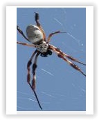
Now the team, led by Dr Zengbo Wang and in colloboration with Prof. Fritz Vollrath’s silk group at Oxford University’s Department of Zoology, has used a naturally occurring material – dragline silk of the golden web spider, as an additional superlens, applied to the surface of the material to be viewed, to provide an additional 2-3 times magnification.
SEM image of Blu-ray disk with 200/100 nm groove and lines (detail). SEM image of Blu-ray disk with 200/100 nm groove and lines (detail).This is the first time that a naturally occurring biological material has been used as a superlens.
In the paper in Nano Letters (DOI: 10.1021/acs.nanolett.6b02641, Aug 17 2016), the joint team reveals how they used a cylindrical piece of spider silk from the thumb sized Nephila spider as a lens.
Dr Zengbo Wang said:
“We have proved that the resolution barrier of microscope can be broken using a superlens, but production of manufactured superlenses invovles some complex engineering processes which are not widely accessible to other reserchers. This is why we have been interested in looking for naturally occurring superlenses provided by ‘Mother Nature’, which may exist around us, so that everyone can access superlenses.”
Prof Fritz Vollrath adds:
“It is very exciting to find yet another cutting edge and totally novel use for a spider silk, which we have been studying for over two decades in my laboratory.”
These lenses could be used for seeing and viewing previously ‘invisible’ structures, including engineered nano-structures and biological micro-structures as well as, potentially, native germs and viruses.
Clear magnified image (2.1x) of Blu-ray disk under spider silk superlens (detail). Clear magnified image (2.1x) of Blu-ray disk under spider silk superlens (detail). The natural cylindrical structure at a micron- and submicron-scale make silks ideal candidates, in this case, the individual filaments had diameters of one tenth of a thin human hair.
The spider filament enabled the group to view details on a micro-chip and a blue- ray disk which would be invisible using the unmodified optical microscope.
In much the same was as when you look through a cylindrical glass or bottle, the clearest image only runs along the narrow strip directly opposite your line of vision, or resting on the surface being viewed, the single filament provides a one dimensional viewing image along its length.
Wang explains:
“The cylindrical silk lens has advantages in the larger field-of-view when compared to a microsphere superlens. Importantly for potential commercial applications, a spider silk nanoscope would be robust and economical, which in turn could provide excellent manufacturing platforms for a wide range of applications.”
James Monks, a co-author on the paper comments: “it has been an exciting time to be able to develop this project as part of my honours degree in electronic engineering at Bangor University and I am now very much looking forward to joining Dr Wang’s team as a PhD student in nano-photonics.”
Share on:


Testimonial
"In a year when every marketing dollar mattered, I chose to keep I-Connect007 in our 2025 plan. Their commitment to high-quality, insightful content aligns with Koh Young’s values and helps readers navigate a changing industry. "
Brent Fischthal - Koh YoungSuggested Items
Electra’s ElectraJet EMJ110 Inkjet Soldermask Now in Black & Blue at Sunrise Electronics
09/08/2025 | Electra Polymers LtdFollowing the successful deployment of Electra’s Green EMJ110 Inkjet Soldermask on KLA’s Orbotech Neos™ platform at Sunrise Electronics in Elk Grove Village, Illinois, production has now moved beyond green.
Magnachip Semiconductor Announces YJ Kim to Step Down as CEO; Current Board Chairman Camillo Martino Appointed Interim CEO
08/14/2025 | PR NewswireMagnachip Semiconductor Corporation today announced that YJ Kim has agreed to step down as CEO and as a member of the Board of Directors, effective immediately. Camillo Martino, Chairman of the Board of Directors, has also been appointed Interim Chief Executive Officer, effective immediately.
Bell to Build X-Plane for Phase 2 of DARPA Speed and Runway Independent Technologies (SPRINT) X-Plane Program
07/09/2025 | Bell Textron Inc.Bell Textron Inc., a Textron Inc. company, has been down-selected for Phase 2 of Defense Advanced Research Projects Agency (DARPA) Speed and Runway Independent Technologies (SPRINT) X-Plane program with the objective to complete design, construction, ground testing and certification of an X-plane demonstrator.
Nolan’s Notes: Moving Forward With Confidence
06/03/2025 | Nolan Johnson -- Column: Nolan's NotesWe’re currently enjoying a revitalized and dynamic EMS provider market with significant growth potential. Since December 2024, the book-to-bill has been extremely strong and growing. Starting with a ratio of 1.24 in December, book-to-bill has continued to accelerate to a 1.41 in April. Yet, there is a global economic restructuring taking place. To say that the back-and-forth with tariffs and trade deals makes for an uncertain market is an understatement. While we may be in a 90-day tariff pause among leading economic nations, the deadline is quickly approaching and that leaves many of you feeling unsettled about what to expect.
Mycronic High Flex Changes Division Name to PCB Assembly Solutions
05/20/2025 | MycronicMycronic AB, the leading Sweden-based electronics assembly solutions provider, announced that its division formerly known as High Flex will now operate under the name PCB Assembly Solutions.