


 Dan’s Biz Bookshelf: Four Important Books You Need to Read (Not Just Say You Have)
 The Marketing Minute: Cracking the Code of Technical Marketing


Measuring Tiny Forces with Light
August 25, 2016 | NISTEstimated reading time: 6 minutes
Photons are bizarre: They have no mass, but they do have momentum. And that allows researchers to do counterintuitive things with photons, such as using light to push matter around.
Recently, a group of scientists led by chemist Gordon Shaw at NIST’s Physical Measurement Laboratory (PML) has been taking advantage of this property to develop devices that can create and measure minute forces, an area traditionally underserved by the metrology community.
“There are very few references for these small forces,” Shaw says. “This is a way to try and get at those.”
When Shaw says “small,” he means small. The official SI unit of force is the newton. One newton is equivalent to about the weight of an average-sized apple. The experiments the group is working on can measure forces that are tiny fractions of a newton – from micronewtons (10 -6, millionths of a newton) all the way down to 15 femtonewtons (10 -15, a million billionth of a newton), at the level of atomic interactions. A piconewton (10 -12) “will stretch a DNA molecule out,” Shaw says.
The PML team is currently developing two types of force-measurement devices that use laser light to reliably create small forces. The first is a chip-sized sensor that can use micro- to milliwatt- power light. The second is a tabletop contraption designed for laser light of about 1 watt, but which could potentially be developed for light of tens of kilowatts of power.
Eventual commercial uses could include sensors that use laser light as a built-in reference, allowing scientists to ensure their devices really are measuring force correctly. But the potential applications go beyond force, into cheap field-portable balances for near-instant measurement of masses of a milligram or less, and into compact laser power meters that make their measurements in real time.
A Chip-Sized Balance
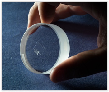
The smaller of the two types of force meter being developed by the team is a chip-sized sensor made of fused quartz. It consists of a small cantilever – a miniature diving board – less than 1 cm in length. The bigger the force, the more the cantilever moves. A built-in interferometer acts as a motion sensor. (For a demonstration, see animation above.)
Chip-sized small force sensor
PML researcher Gordon Shaw holding a prototype for the chip-sized small-force meter. The cantilever is near the intersection of the two rectangles in the center of the glass cylinder.
Physically pushing the diving board is one way to apply a force for measurement. But researchers also need to gauge the sensitivity of their sensor. And the best way to measure sensitivity is to apply a well-known force to the cantilever and see how the interferometer interprets it.
To manipulate the cantilever with light, they fit it with a highly reflective, gold-coated surface that can reflect light shining on it from an optical fiber. When this light hits the gold surface, it transfers its momentum to the cantilever, which begins to vibrate.
“If you think of a tuning fork, you can hit it and it will ring at a particular frequency or a particular tone. This does the same thing,” Shaw explains.
They found that if you reflect laser light off the surface, there’s a relatively straightforward way to calculate what the force should be based on the laser power. The higher the power, the more photons there are, and the larger the force that’s generated.
Furthermore, since the cantilever’s resonant frequency changes almost instantly if a mass is placed on it, the mechanism could also be used as a very sensitive balance – particularly for objects that are extremely valuable or dangerous. For example, jewelers could use it as a less expensive alternative for weighing and pricing gemstones. It could even be used potentially as a field-portable, disposable tool for measuring samples of hazardous materials.
Variations on this design could also be used to improve calibrations of atomic force microscopes* and even to measure laser power. Unlike the current “gold standard” method of measuring laser power – a cryogenic radiometer – a chip-based laser power meter like this can be used at room temperature and in real time.
“Most laser power meters work by absorbing the light. After the light goes to the laser power meter, it’s gone,” Shaw says. “With an approach like this, it reflects and you can still use it.”
Page 1 of 2
Share on:


Testimonial
"The I-Connect007 team is outstanding—kind, responsive, and a true marketing partner. Their design team created fresh, eye-catching ads, and their editorial support polished our content to let our brand shine. Thank you all! "
Sweeney Ng - CEE PCBSuggested Items
Trouble in Your Tank: Implementing Direct Metallization in Advanced Substrate Packaging
09/15/2025 | Michael Carano -- Column: Trouble in Your TankDirect metallization systems based on conductive graphite are gaining popularity throughout the world. The environmental and productivity gains achievable with this process are outstanding. Direct metallization reduces the costs of compliance, waste treatment, and legal issues related to chemical exposure. A graphite-based direct plate system has been devised to address these needs.
Closing the Loop on PCB Etching Waste
09/09/2025 | Shawn Stone, IECAs the PCB industry continues its push toward greener, more cost-efficient operations, Sigma Engineering’s Mecer System offers a comprehensive solution to two of the industry’s most persistent pain points: etchant consumption and rinse water waste. Designed as a modular, fully automated platform, the Mecer System regenerates spent copper etchants—both alkaline and acidic—and simultaneously recycles rinse water, transforming a traditionally linear chemical process into a closed-loop system.
Driving Innovation: Depth Routing Processes—Achieving Unparalleled Precision in Complex PCBs
09/08/2025 | Kurt Palmer -- Column: Driving InnovationIn PCB manufacturing, the demand for increasingly complex and miniaturized designs continually pushes the boundaries of traditional fabrication methods, including depth routing. Success in these applications demands not only on robust machinery but also sophisticated control functions. PCB manufacturers rely on advanced machine features and process methodologies to meet their precise depth routing goals. Here, I’ll explore some crucial functions that empower manufacturers to master complex depth routing challenges.
Trouble in Your Tank: Minimizing Small-via Defects for High-reliability PCBs
08/27/2025 | Michael Carano -- Column: Trouble in Your TankTo quote the comedian Stephen Wright, “If at first you don’t succeed, then skydiving is not for you.” That can be the battle cry when you find that only small-diameter vias are exhibiting voids. Why are small holes more prone to voids than larger vias when processed through electroless copper? There are several reasons.
The Government Circuit: Navigating New Trade Headwinds and New Partnerships
08/25/2025 | Chris Mitchell -- Column: The Government CircuitAs global trade winds continue to howl, the electronics manufacturing industry finds itself at a critical juncture. After months of warnings, the U.S. Government has implemented a broad array of tariff increases, with fresh duties hitting copper-based products, semiconductors, and imports from many nations. On the positive side, tentative trade agreements with Europe, China, Japan, and other nations are providing at least some clarity and counterbalance.