


 Dan’s Biz Bookshelf: Four Important Books You Need to Read (Not Just Say You Have)
 The Marketing Minute: Cracking the Code of Technical Marketing


Meteorite Impact on a Nano Scale
August 29, 2016 | Vienna University of TechnologyEstimated reading time: 5 minutes
A meteorite impacting the earth under a grazing angle of incidence can do a lot of damage; it may travel a long way, carving a trench into the ground until it finally penetrates the surface. The impact site may be vaporized, there can be large areas of molten ground. All that remains is a crater, some debris, and an extensive trail of devastation on both sides of the impact site.
Hitting a surface with high-energy, heavy ions has quite similar effects - only on a much smaller scale. At TU Wien (Vienna), Prof. Friedrich Aumayr and his team have been studying the microscopic structures which are formed when ions are fired at crystals at oblique angles of incidence.
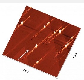
Trenches and Ridges
"When we take a look at the crystal surface with an atomic force microscope, we can clearly see the similarities between ion impacts and meteorite impacts", says Elisabeth Gruber, PhD-student in Friedrich Aumayrs team. "At first the projectile, scratching across the surface at a grazing angle, digs a trench into the crystal surface, which can be hundreds of nanometers long. Extensive ridges appear on either side of the trench, consisting of tiny structures called nanohillocks." When the projectile ultimately enters the crystal and disappears, an especially large hillock is created at the impact site. Beyond that, the ion keeps moving below the surface, until it finally comes to a halt.
This may sound simple and obvious, as if high energy ions just behaved like tiny, electrically charged bullets. But in fact, it is not at all self-evident that objects on a nano scale behave like macroscopic objects do. When atoms exchange energy, quantum physics always plays an important role.
"When the high-energy ions interact with crystal surfaces - calcium fluoride, in our case - many different physical effects have to be taken into account", says Friedrich Aumayr. "Electrons can change their energy state, they can exchange energy with atoms around them and excite vibrations in the crystal lattice, the so-called phonons. We have to carefully consider all these effects when we want to understand how the nanostructures on the crystal surface are created."
Melting and Evaporation
In order to understand the mechanism leading to the nano-trenches and hillocks, the team developed extensive computer simulations, together with colleagues from Germany. "That way we can determine, how much different parts of the crystal surface are heated up", says Elisabeth Gruber. "There are regions which become so hot that the material melts, at certain points it can even evaporate. When we know how large these regions are, we can predict very accurately what the nanostructures on the crystal surface will look like."
The goal of this line of research is not only to understand how tailored nanostructures can be created. It is also important to find out how different materials are harmed by heavy ion bombardment. "Calcium fluoride is often used as an insulator in semiconductor technology", says Friedrich Aumayr. "We want our electronics to work, even under extreme conditions, for instance in a satellite which is exposed to cosmic radiation." When the calcium fluoride layer is riddled with tiny holes, it can cause the device to short circuit and fail. Therefore, it is vital to understand the interaction of crystal surfaces and fast ions.
Hitting a surface with high-energy, heavy ions has quite similar effects - only on a much smaller scale. At TU Wien (Vienna), Prof. Friedrich Aumayr and his team have been studying the microscopic structures which are formed when ions are fired at crystals at oblique angles of incidence.
Trenches and Ridges
"When we take a look at the crystal surface with an atomic force microscope, we can clearly see the similarities between ion impacts and meteorite impacts", says Elisabeth Gruber, PhD-student in Friedrich Aumayrs team. "At first the projectile, scratching across the surface at a grazing angle, digs a trench into the crystal surface, which can be hundreds of nanometers long. Extensive ridges appear on either side of the trench, consisting of tiny structures called nanohillocks." When the projectile ultimately enters the crystal and disappears, an especially large hillock is created at the impact site. Beyond that, the ion keeps moving below the surface, until it finally comes to a halt.
This may sound simple and obvious, as if high energy ions just behaved like tiny, electrically charged bullets. But in fact, it is not at all self-evident that objects on a nano scale behave like macroscopic objects do. When atoms exchange energy, quantum physics always plays an important role.
"When the high-energy ions interact with crystal surfaces - calcium fluoride, in our case - many different physical effects have to be taken into account", says Friedrich Aumayr. "Electrons can change their energy state, they can exchange energy with atoms around them and excite vibrations in the crystal lattice, the so-called phonons. We have to carefully consider all these effects when we want to understand how the nanostructures on the crystal surface are created."
Melting and Evaporation
In order to understand the mechanism leading to the nano-trenches and hillocks, the team developed extensive computer simulations, together with colleagues from Germany. "That way we can determine, how much different parts of the crystal surface are heated up", says Elisabeth Gruber. "There are regions which become so hot that the material melts, at certain points it can even evaporate. When we know how large these regions are, we can predict very accurately what the nanostructures on the crystal surface will look like."
The goal of this line of research is not only to understand how tailored nanostructures can be created. It is also important to find out how different materials are harmed by heavy ion bombardment. "Calcium fluoride is often used as an insulator in semiconductor technology", says Friedrich Aumayr. "We want our electronics to work, even under extreme conditions, for instance in a satellite which is exposed to cosmic radiation." When the calcium fluoride layer is riddled with tiny holes, it can cause the device to short circuit and fail. Therefore, it is vital to understand the interaction of crystal surfaces and fast ions.
Share on:


Testimonial
"We’re proud to call I-Connect007 a trusted partner. Their innovative approach and industry insight made our podcast collaboration a success by connecting us with the right audience and delivering real results."
Julia McCaffrey - NCAB GroupSuggested Items
Driving Innovation: Depth Routing Processes—Achieving Unparalleled Precision in Complex PCBs
09/08/2025 | Kurt Palmer -- Column: Driving InnovationIn PCB manufacturing, the demand for increasingly complex and miniaturized designs continually pushes the boundaries of traditional fabrication methods, including depth routing. Success in these applications demands not only on robust machinery but also sophisticated control functions. PCB manufacturers rely on advanced machine features and process methodologies to meet their precise depth routing goals. Here, I’ll explore some crucial functions that empower manufacturers to master complex depth routing challenges.
Polar Instruments Announces Additive Transmission Line Support for Si9000e
08/20/2025 | Polar InstrumentsTransmission lines embedded into the PCB surface are a feature of UHDI constructions. The 2025 fall release of Polar's Si9000e PCB impedance & insertion loss transmission line field solver incorporates eight new single ended, differential and coplanar transmission line structures.
Henniker Plasma Launches Stratus Turnkey Plasma Manufacturing Cell
08/13/2025 | Henniker PlasmaHenniker Plasma, a leading manufacturer of plasma treatment systems, proudly announces the launch of its Stratus Plasma Manufacturing Cell range — a fully integrated, turnkey solution that combines advanced atmospheric plasma surface treatment with robotic automation.
Trouble in Your Tank: Metallizing Flexible Circuit Materials—Mitigating Deposit Stress
08/04/2025 | Michael Carano -- Column: Trouble in Your TankMetallizing materials, such as polyimide used for flexible circuitry and high-reliability multilayer printed wiring boards, provide a significant challenge for process engineers. Conventional electroless copper systems often require pre-treatments with hazardous chemicals or have a small process window to achieve uniform coverage without blistering. It all boils down to enhancing the adhesion of the thin film of electroless copper to these smooth surfaces.
Designers Notebook: Basic PCB Planning Criteria—Establishing Design Constraints
07/22/2025 | Vern Solberg -- Column: Designer's NotebookPrinted circuit board development flows more smoothly when all critical issues are predefined and understood from the start. As a basic planning strategy, the designer must first consider the product performance criteria, then determine the specific industry standards or specifications that the product must meet. Planning also includes a review of all significant issues that may affect the product’s manufacture, performance, reliability, overall quality, and safety.