


 The Marketing Minute: Cracking the Code of Technical Marketing
 Trouble in Your Tank: Implementing Direct Metallization in Advanced Substrate Packaging


Subatomic Microscopy Key to Building New Classes of Materials
September 1, 2016 | Pennsylvania State UniversityEstimated reading time: 3 minutes
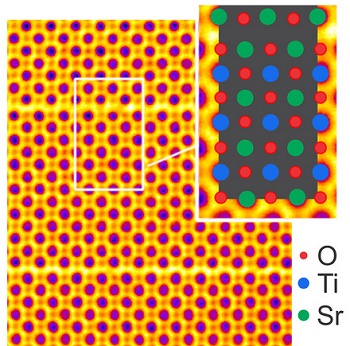
Researchers at Penn State and the Molecular Foundry at Lawrence Berkeley National Laboratory are pushing the limits of electron microscopy into the tens of picometer scale, a fraction of the size of a hydrogen atom.
The ability to see at this subatomic level is crucial for designing new materials with unprecedented properties, such as materials that transition from metals to semiconductors or that exhibit superconductivity. The researchers' work describing the first atomic scale evidence for strain-induced ferroelectricity in a layered oxide appears online today, (Aug. 31), in Nature Communications.
"This paper is important because it highlights our ability to design new classes of materials that can be tuned, one atomic layer at a time, to get interesting new properties such as high-frequency tunable dielectrics, which are of interest to the semiconductor industry," said first author Greg Stone, a former Penn State post-doctoral scholar now at the U.S. Army Research, Development, and Engineering Center.
Designing new materials with potentially useful properties requires the close collaboration of theory, synthesis and characterization – the first to build the mathematical models needed, the second to create the material in the lab, and the third to visualize and measure the material's properties and provide feedback to tweak theories and improve synthesis.
This study builds on previous theoretical work by coauthors Turan Birol and Craig Fennie of Cornell University and experimental work by coauthors Venkatraman Gopalan of Penn State and Darrell Schlom, formerly at Penn State and now at Cornell, and their students. Gopalan and Nasim Alem, professors of materials science and engineering at Penn State, led the current study.
"The material we are looking at is a form of strontium titanate called a layered oxide," said Gopalan. "This study brings together electron microscopy and density functional theory on a 5 to 10 picometer length scale to show why these materials are such good tunable dielectrics. The key is phase competition, and for the first time, we show that many polar phases with similar energies compete in this material on the atomic scale, just as theory predicted, which gives it large tunability under a voltage."
Complex oxides are materials that form by combining negatively charged oxygen and two other positively charged ions. In this instance, the team examined strontium titanate with a structure called Ruddlesden-Popper (RP), after the two scientists who discovered it. The structure looks like a brick and mortar wall, with the bricks made of the strontium titanate and the thin mortar between the bricks made up of strontium oxide. When the bricks are layered in this fashion, new properties emerge that would not appear in a single brick.
"In the case of RP-strontium titanate, the emergent property is ferroelectricity, which means it has a built-in electrical polarization within its structure," said Gopalan. "But it could be magnetism or metal-insulator transitions or superconductivity, depending on the atoms involved and the layering order of the materials."
Because each layer of brick has a weak connection to other layers, the material can have competing states, with one layer polarized in a direction opposite to a neighboring layer. These competing states result in a material with a strong response to a small external stimulus, such as an electric or magnetic field or temperature. In the case of strontium titanate, there is a large dielectric response, which is the ability to store large amounts of energy, as in a capacitor.
Cell phones have many dielectric components that are very small and have to hold a charge. As cell phones transition from 4G networks to 5G, which means they are processing at 5 billion cycles per second, better materials that respond at higher frequencies are crucial. RP-strontium titanate is a material that is definitely superior to current materials.
Colin Ophus of the National Center for Electron Microscopy facility of the Molecular Foundry, said, "This work is an excellent example of the materials advances possible when we close the feedback loop between first principles calculations and atomic resolution electron microscopy."
His colleague Jim Ciston at the Molecular Foundry adds, "The precision of the agreement between theory and experiment is critical to unraveling the subtle differences in structure between competing ferroelectric phases. These images of atomic positions are more than pretty pictures of remarkable precision, but contain an enormous amount of quantifiable information about the minute distortions in atomic positions that can lead to surprising properties."
Additional coauthors on the paper, titled "Atomic Scale Imaging of Competing Polar States in a Ruddleston-Popper Layered Oxide," were Nasim Alem, assistant professor of materials science and engineering, Penn State, Turan Birol, Fennie's Ph.D. student now assistant professor at University of Minnesota, Che-Hui Lee, Schlom's Ph.D. student at Penn State and Cornell, and Penn State staff scientist Ke Wang.
Share on:


Testimonial
"Advertising in PCB007 Magazine has been a great way to showcase our bare board testers to the right audience. The I-Connect007 team makes the process smooth and professional. We’re proud to be featured in such a trusted publication."
Klaus Koziol - atgSuggested Items
Curing and Verification in PCB Shadow Areas
09/17/2025 | Doug Katze, DymaxDesign engineers know a simple truth that often complicates electronics manufacturing: Light doesn’t go around corners. In densely populated PCBs, adhesives and coatings often fail to fully cure in shadowed regions created by tall ICs, connectors, relays, and tight housings.
Marcy’s Musings: Advancing the Advanced Materials Discussion
09/17/2025 | Marcy LaRont -- Column: Marcy's MusingsAs the industry’s most trusted global source of original content about the electronics supply chain, we continually ask you about your concerns, what you care about, and what you most want to learn about. Your responses are insightful and valuable. Thank you for caring enough to provide useful feedback and engage in dialogue.
September 2025 PCB007 Magazine: The Future of Advanced Materials
09/16/2025 | I-Connect007 Editorial TeamMoore’s Law is no more, and the advanced material solutions being developed to grapple with this reality are surprising, stunning, and perhaps a bit daunting. Buckle up for a dive into advanced materials and a glimpse into the next chapters of electronics manufacturing.
I-Connect007 Launches Advanced Electronics Packaging Digest
09/15/2025 | I-Connect007I-Connect007 is pleased to announce the launch of Advanced Electronics Packaging Digest (AEPD), a new monthly digital newsletter dedicated to one of the most critical and rapidly evolving areas of electronics manufacturing: advanced packaging at the interconnect level.
Panasonic Industry will Double the Production Capacity of MEGTRON Multi-layer Circuit Board Materials Over the Next Five Years
09/15/2025 | Panasonic Industry Co., Ltd.Panasonic Industry Co., Ltd., a Panasonic Group company, announced plans for a major expansion of its global production capacity for MEGTRON multi-layer circuit board materials today. The company plans to double its production over the next five years to meet growing demand in the AI server and ICT infrastructure markets.