


 Punching Out: How to Stay Focused in Business and M&A
 It’s Only Common Sense: Just Imagine…


Last March, the artificial intelligence (AI) program AlphaGo beat Korean Go champion LEE Se-Dol at the Asian board game. "The game was quite tight, but AlphaGo used 1200 CPUs and 56,000 watts per hour, while Lee used only 20 watts. If a hardware that mimics the human brain structure is developed, we can operate artificial intelligence with less power," points out Professor YU Woo Jong. In collaboration with Sungkyunkwan University, researchers from the Center for Integrated Nanostructure Physics within the Institute for Basic Science (IBS), have devised a new memory device inspired by the neuron connections of the human brain. The research, published in Nature Communications, highlights the device’s highly reliable performance, long retention time and endurance. Moreover, its stretchability and flexibility makes it a promising tool for the next-generation soft electronics attached to clothes or body.
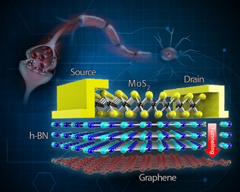
The brain is able to learn and memorize thanks to a huge number of connections between neurons. The information you memorize is transmitted through synapses from one neuron to the next as an electro-chemical signal. Inspired by these connections, IBS scientists constructed a memory called two-terminal tunnelling random access memory (TRAM), where two electrodes, referred to as drain and source, resemble the two communicating neurons of the synapse. While mainstream mobile electronics, like digital cameras and mobile phones use the so-called three-terminal flash memory, the advantage of two-terminal memories like TRAM is that two-terminal memories do not need a thick and rigid oxide layer. "Flash memory is still more reliable and has better performance, but TRAM is more flexible and can be scalable," explains Professor Yu.
TRAM is made up of a stack of one-atom-thick or a few atom-thick 2D crystal layers: One layer of the semiconductor molybdenum disulfide (MoS2) with two electrodes (drain and source), an insulating layer of hexagonal boron nitride (h-BN) and a graphene layer. In simple terms, memory is created (logical-0), read and erased (logical-1) by the flowing of charges through these layers. TRAM stores data by keeping electrons on its graphene layer. By applying different voltages between the electrodes, electrons flow from the drain to the graphene layer tunnelling through the insulating h-BN layer. The graphene layer becomes negatively charged and memory is written and stored and vice versa, when positive charges are introduced in the graphene layer, memory is erased.
In the junctions (synapses) between neurons, signals are transmitted from one neuron to the next. TRAM is made by a stack of different layers: A semiconductor molybdenum disulfide (MoS2) layer with two electrodes (drain and source), an insulating hexagonal boron nitride (h-BN) layer and graphene layer. This two-terminal architecture simulates the two neurons that made up to the synaptic structure. When the difference in the voltage of the drain and the source is sufficiently high, electrons from the drain electrode tunnel through the insulating h-BN and reach the graphene layer. Memory is written when electrons are stored in the graphene layer, and it is erased by the introduction of positive charges in the graphene layer.
IBS scientists carefully selected the thickness of the insulating h-BN layer as they found that a thickness of 7.5 nanometers allows the electrons to tunnel from the drain electrode to the graphene layer without leakages and without losing flexibility.
The appropriate thickness of the h-BN isolating layers allows electrons to tunnel and reach the graphene layer without leakages. H-BN layers of different thicknesses were tested and a thickness of 7.5 nanometers was found to be the most appropriate.
Flexibility and stretchability are indeed two key features of TRAM. When TRAM was fabricated on flexible plastic (PET) and stretachable silicone materials (PDMS), it could be strained up to 0.5% and 20%, respectively. In the future, TRAM can be useful to save data from flexible or wearable smartphones, eye cameras, smart surgical gloves, and body-attachable biomedical devices.
Two-terminal tunnelling random access memory (TRAM) shows good flexibility when built on flexible polyethylene terephthalate (PET). TRAM can be useful for next-generation wearable or body-attachable soft devices.
Last but not least, TRAM has better performance than other types of two-terminal memories known as phase-change random-access memory (PRAM) and resistive random-access memory (RRAM).
TRAM overcomes the limitations of other types of two-terminal memories. TRAM has better performance - that is higher on/off ratio - than other types of two-terminal memories called PRAM and RRAM. The on/off ratio is the difference between the on-state current and off-state current. The higher this difference; the better the performance of the memory.


