


 Dan’s Biz Bookshelf: Four Important Books You Need to Read (Not Just Say You Have)
 The Marketing Minute: Cracking the Code of Technical Marketing


Rutgers Engineers Use Microwaves to Produce High-Quality Graphene
September 5, 2016 | Rutgers UniversityEstimated reading time: 1 minute
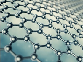
Rutgers University engineers have found a simple method for producing high-quality graphene that can be used in next-generation electronic and energy devices: bake the compound in a microwave oven.
The discovery is documented in a study published online today in the journal Science.
“This is a major advance in the graphene field,” said Manish Chhowalla, professor and associate chair in the Department of Materials Science and Engineering in Rutgers’ School of Engineering. “This simple microwave treatment leads to exceptionally high quality graphene with properties approaching those in pristine graphene.”
The discovery was made by post-doctoral associates and undergraduate students in the department, said Chhowalla, who is also the director of the Rutgers Institute for Advanced Materials, Devices and Nanotechnology. Having undergraduates as co-authors of a Science paper is rare but he said “the Rutgers Materials Science and Engineering Department and the School of Engineering at Rutgers cultivate a culture of curiosity driven research in students with fresh ideas who are not afraid to try something new.’’
Graphene – 100 times tougher than steel – conducts electricity better than copper and rapidly dissipates heat, making it useful for many applications. Large-scale production of graphene is necessary for applications such as printable electronics, electrodes for batteries and catalysts for fuel cells.
Graphene comes from graphite, a carbon-based material used by generations of students and teachers in the form of pencils. Graphite consists of sheets or layers of graphene.
The easiest way to make large quantities of graphene is to exfoliate graphite into individual graphene sheets by using chemicals. The downside of this approach is that side reactions occur with oxygen – forming graphene oxide that is electrically non-conducting, which makes it less useful for products.
Removing oxygen from graphene oxide to obtain high-quality graphene has been a major challenge over the past two decades for the scientific community working on graphene. Oxygen distorts the pristine atomic structure of graphene and degrades its properties.
Chhowalla and his group members found that baking the exfoliated graphene oxide for just one second in a 1,000-watt microwave oven, like those used in households across America, can eliminate virtually all of the oxygen from graphene oxide.
Share on:


Testimonial
"We’re proud to call I-Connect007 a trusted partner. Their innovative approach and industry insight made our podcast collaboration a success by connecting us with the right audience and delivering real results."
Julia McCaffrey - NCAB GroupSuggested Items
Trouble in Your Tank: Implementing Direct Metallization in Advanced Substrate Packaging
09/15/2025 | Michael Carano -- Column: Trouble in Your TankDirect metallization systems based on conductive graphite are gaining popularity throughout the world. The environmental and productivity gains achievable with this process are outstanding. Direct metallization reduces the costs of compliance, waste treatment, and legal issues related to chemical exposure. A graphite-based direct plate system has been devised to address these needs.
Closing the Loop on PCB Etching Waste
09/09/2025 | Shawn Stone, IECAs the PCB industry continues its push toward greener, more cost-efficient operations, Sigma Engineering’s Mecer System offers a comprehensive solution to two of the industry’s most persistent pain points: etchant consumption and rinse water waste. Designed as a modular, fully automated platform, the Mecer System regenerates spent copper etchants—both alkaline and acidic—and simultaneously recycles rinse water, transforming a traditionally linear chemical process into a closed-loop system.
Driving Innovation: Depth Routing Processes—Achieving Unparalleled Precision in Complex PCBs
09/08/2025 | Kurt Palmer -- Column: Driving InnovationIn PCB manufacturing, the demand for increasingly complex and miniaturized designs continually pushes the boundaries of traditional fabrication methods, including depth routing. Success in these applications demands not only on robust machinery but also sophisticated control functions. PCB manufacturers rely on advanced machine features and process methodologies to meet their precise depth routing goals. Here, I’ll explore some crucial functions that empower manufacturers to master complex depth routing challenges.
Trouble in Your Tank: Minimizing Small-via Defects for High-reliability PCBs
08/27/2025 | Michael Carano -- Column: Trouble in Your TankTo quote the comedian Stephen Wright, “If at first you don’t succeed, then skydiving is not for you.” That can be the battle cry when you find that only small-diameter vias are exhibiting voids. Why are small holes more prone to voids than larger vias when processed through electroless copper? There are several reasons.
The Government Circuit: Navigating New Trade Headwinds and New Partnerships
08/25/2025 | Chris Mitchell -- Column: The Government CircuitAs global trade winds continue to howl, the electronics manufacturing industry finds itself at a critical juncture. After months of warnings, the U.S. Government has implemented a broad array of tariff increases, with fresh duties hitting copper-based products, semiconductors, and imports from many nations. On the positive side, tentative trade agreements with Europe, China, Japan, and other nations are providing at least some clarity and counterbalance.