


 Dan’s Biz Bookshelf: Four Important Books You Need to Read (Not Just Say You Have)
 The Marketing Minute: Cracking the Code of Technical Marketing


New Computer Chip Manufacturing Method Squeezes More onto Limited Wafer Space
September 9, 2016 | University of Wisconsin-MadisonEstimated reading time: 3 minutes
Computer chip makers continuously strive to pack more transistors in less space, yet as the size of those transistors approaches the atomic scale, there are physical limits on how small they are able to make the patterns for the circuitry.
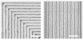
Scanning electron micrographs of block copolymer films assembled on graphene/germanium chemical patterns with 90 degree bends (left side) and with density multiplication by a factor of 10 (right side). The black dotted lines (right side) indicate the period of the graphene/germanium chemical pattern, in which the period of the assembled block copolymer is reduced by a factor of 10 due to density multiplication. The scale bars are 200 nm.
Now, taking advantage of a germanium wafer coated with a layer of virtually pristine graphene — a sheet of carbon arranged just one atom thick — a team of engineers from the University of Wisconsin–Madison and the University of Chicago has devised a simpler, reproducible and less expensive manufacturing approach using directed self-assembly.
Directed self-assembly is a large-scale, nano-patterning technique that can increase the density of circuit patterns and circumvent some limitations of conventional lithographic processes for printing circuits on wafers of semiconductors such as silicon.
Electrical engineer Zhenqiang “Jack” Ma and materials engineer Michael Arnold of UW–Madison, chemical engineer Paul Nealey of the University of Chicago, and their students published details of the advance in the Aug. 16 edition of the journal Scientific Reports.
Their work could mean a boost in functionality for semiconductor electronics and in capacity for data storage.
To achieve the incredibly tiny size required for the circuitry in future semiconductor electronics, manufacturers are developing directed self-assembly, which enables the fabrication of intricate, perfectly ordered polymer patterns for circuitry.
Chemical patterns consisting of alternating graphene and germanium stripes (left side) are used to direct the self-assembly of block copolymers into well-ordered patterns (right side). The top images are schematics and the bottom images are scanning electron micrographs. The scale bars are 200 nm.
For directed self-assembly, the researchers use conventional chemical techniques to define a pre-pattern. When chains of molecules known as block copolymers self-assemble on the pre-pattern, they follow the pattern to form well-ordered features.
The researchers’ new method is much faster, and reduces the number of steps in the process to just two: lithography and plasma etching.
In the first demonstration of their technique, the researchers used electron beam lithography and a mild plasma etching technique to pattern one-atom-thick graphene stripes on a germanium wafer. Then they spin-coated the wafer with a common block copolymer called polystyrene-block-poly(methyl methacrylate).
When heated, the block copolymer self-assembled completely in just 10 minutes — compared to 30 minutes using conventional chemical patterns — and with fewer defects. The researchers attribute this rapid assembly to the smooth, rigid, crystalline surfaces of germanium and graphene.
Their new method takes advantage of a phenomenon called density multiplication. The researchers used electron beam lithography to first create a larger master template with sparse patterns that guide the orientation of their block copolymers.
When they directed the block copolymer to self-assemble, it did so in a way that enhanced the resolution of the original template — in this case, by a factor of 10. The best previous enhancement by density multiplication was a factor of four.
While the stripe pattern was a simple demonstration of their technique, the researchers also showed it works with more architecturally complex or irregular patterns, including those with abrupt 90-degree bends.
“These templates offer an exciting alternative to traditional chemical patterns composed of polymer mats and brushes, as they provide faster assembly kinetics and broaden the processing window, while also offering an inert, mechanically and chemically robust, and uniform template with well defined and sharp material interfaces,” says Nealey.
The technique enables them to combine the uniformity and simpler processing of traditional “top-down” lithographic methods with the advantages of “bottom-up” assembly and greater density multiplication, and offers a promising route for large-scale production at significantly reduced cost.
“Using this one-atom-thick graphene template has never been done before. It’s a new template to guide the self-assembly of the polymers,” says Ma. “This is mass-production-compatible. We opened the door to even smaller features.”
The researchers are patenting their method through the Wisconsin Alumni Research Foundation. Funding from the U.S. departments of Energy and Defense, UW–Madison and the University of Chicago supported their work.
Other authors on the paper include Tzu-Hsuan Chang, Robert M. Jacobberger, Solomon Mikael, Dalong Geng and Xudong Wang of UW–Madison, and Shisheng Xiong, Hyo Seon Suh and Chi-Chun Liu of the University of Chicago.
Share on:


Testimonial
"Advertising in PCB007 Magazine has been a great way to showcase our bare board testers to the right audience. The I-Connect007 team makes the process smooth and professional. We’re proud to be featured in such a trusted publication."
Klaus Koziol - atgSuggested Items
Indium President and CEO to Deliver ELCINA CEO Forum Keynote at Productronica India
09/17/2025 | Indium CorporationIndium Corporation President and CEO Ross Berntson will deliver the Electronic Industries Association of India (ELCINA) CEO Forum keynote at Productronica India, to be held September 17-19 in Bengaluru, India.
Curing and Verification in PCB Shadow Areas
09/17/2025 | Doug Katze, DymaxDesign engineers know a simple truth that often complicates electronics manufacturing: Light doesn’t go around corners. In densely populated PCBs, adhesives and coatings often fail to fully cure in shadowed regions created by tall ICs, connectors, relays, and tight housings.
Variosystems Strengthens North American Presence with Southlake Relaunch 2025
09/15/2025 | VariosystemsVariosystems celebrated the relaunch of its U.S. facility in Southlake, Texas. After months of redesign and reorganization, the opening marked more than just the return to a modernized production site—it was a moment to reconnect with our teams, partners, and the local community.
MacDermid Alpha Presents at SMTA New Delhi, Bangalore Chapter, on Flux–OSP Interaction
09/09/2025 | MacDermid Alpha Electronics SolutionsMacDermid Alpha contributes technical insights on OSP solderability at the Bangalore Chapter, SMTA reinforcing commitment to knowledge-sharing and industry collaboration.
Naprotek Appoints Mark Crebs to Lead Business Development for Products and Platforms
08/27/2025 | Naprotek LLCNaprotek, LLC, a leading provider of mission-critical electronics technology solutions, announced the appointment of Mark Crebs to Products and Platform Director of Business Development.