


 Dan’s Biz Bookshelf: Four Important Books You Need to Read (Not Just Say You Have)
 The Marketing Minute: Cracking the Code of Technical Marketing


Understanding How Flat Phosphorus Grows
September 12, 2016 | A*STAREstimated reading time: 2 minutes
The door to developing superior electronic devices, such as flexible circuits, has been nudged open by A*STAR researchers’ modeling of possible methods to manufacture one of the crucial ingredients.
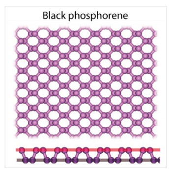
Phosphorene is a two-dimensional (2D) form of the element phosphorus. Despite having electronic properties superior to other 2D materials such as graphene (2D carbon) and silicene (2D silicon), phosphorene’s potential for application in high-performance devices has been limited by how difficult it is to reliably produce commercially viable quantities of it in large, thin, high-quality nanosheet form.
At present, phosphorene can only be obtained by mechanical and chemical exfoliation of black phosphorus, which is costly and produces low yields of uneven films. Other 2D materials such as graphene and molybdenum disulfide can be directly grown using chemical vapor deposition and physical vapor deposition, but no such methods exist for growing phosphorene.
The new model developed by Junfeng Gao and colleagues from the A*STAR Institute of High Performance Computing will make it possible for researchers to tackle this challenging technical problem by choosing the best process conditions for the growth of large-size, high-quality phosphorene directly on a surface.
Gao and the team tried to find the best way to grow high-quality single layers of phophorene directly on a surface by modeling the effect of different substrates on the growth of a phosphorene flake containing just 27 atoms.
“The stability of the growing nanoflake is highly sensitive to the substrate and crucial to its continued growth,” explains Gao. “If the interaction strength is too weak, the substrate causes the flake to buckle; but if the interaction is too strong, the inner bonds between the phosphorene atoms will break and an alloy may form.”
The researchers compared the effect of two different substrates on the growth of the phosphorene nanoflake — a copper substrate, commonly used for growing graphene, which bonds with the phosphorene through strong chemical processes, and a hexagonal hydrogen boron nitride (h-BN) substrate that couples with the phosphorene via weak van der Waals bonds.
The copper substrate caused the nanoflake to break, whereas the h-BN was unable to stabilize its flat structure. By boosting the strength of the bonding between the nanoflake and the h-BN substrate, their simulations showed that the 2D growth of the phosphorene was maintained. “Our work is the first attempt to explore the direct growth of phosphorene and provides guidance in the search for suitable substrates,” says Gao.
Share on:


Testimonial
"In a year when every marketing dollar mattered, I chose to keep I-Connect007 in our 2025 plan. Their commitment to high-quality, insightful content aligns with Koh Young’s values and helps readers navigate a changing industry. "
Brent Fischthal - Koh YoungSuggested Items
Trouble in Your Tank: Implementing Direct Metallization in Advanced Substrate Packaging
09/15/2025 | Michael Carano -- Column: Trouble in Your TankDirect metallization systems based on conductive graphite are gaining popularity throughout the world. The environmental and productivity gains achievable with this process are outstanding. Direct metallization reduces the costs of compliance, waste treatment, and legal issues related to chemical exposure. A graphite-based direct plate system has been devised to address these needs.
Closing the Loop on PCB Etching Waste
09/09/2025 | Shawn Stone, IECAs the PCB industry continues its push toward greener, more cost-efficient operations, Sigma Engineering’s Mecer System offers a comprehensive solution to two of the industry’s most persistent pain points: etchant consumption and rinse water waste. Designed as a modular, fully automated platform, the Mecer System regenerates spent copper etchants—both alkaline and acidic—and simultaneously recycles rinse water, transforming a traditionally linear chemical process into a closed-loop system.
Driving Innovation: Depth Routing Processes—Achieving Unparalleled Precision in Complex PCBs
09/08/2025 | Kurt Palmer -- Column: Driving InnovationIn PCB manufacturing, the demand for increasingly complex and miniaturized designs continually pushes the boundaries of traditional fabrication methods, including depth routing. Success in these applications demands not only on robust machinery but also sophisticated control functions. PCB manufacturers rely on advanced machine features and process methodologies to meet their precise depth routing goals. Here, I’ll explore some crucial functions that empower manufacturers to master complex depth routing challenges.
Trouble in Your Tank: Minimizing Small-via Defects for High-reliability PCBs
08/27/2025 | Michael Carano -- Column: Trouble in Your TankTo quote the comedian Stephen Wright, “If at first you don’t succeed, then skydiving is not for you.” That can be the battle cry when you find that only small-diameter vias are exhibiting voids. Why are small holes more prone to voids than larger vias when processed through electroless copper? There are several reasons.
The Government Circuit: Navigating New Trade Headwinds and New Partnerships
08/25/2025 | Chris Mitchell -- Column: The Government CircuitAs global trade winds continue to howl, the electronics manufacturing industry finds itself at a critical juncture. After months of warnings, the U.S. Government has implemented a broad array of tariff increases, with fresh duties hitting copper-based products, semiconductors, and imports from many nations. On the positive side, tentative trade agreements with Europe, China, Japan, and other nations are providing at least some clarity and counterbalance.