


 The Marketing Minute: Cracking the Code of Technical Marketing
 Trouble in Your Tank: Implementing Direct Metallization in Advanced Substrate Packaging


New Technique Integrates Graphene, GO and rGO onto Silicon Chips at Room Temperature
September 14, 2016 | North Carolina State UniversityEstimated reading time: 1 minute
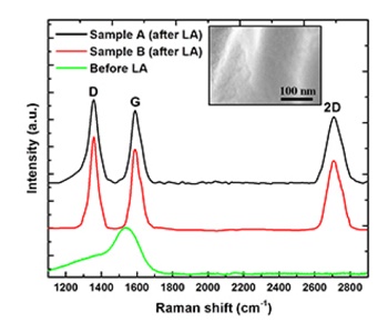
Materials researchers at North Carolina State University have developed a technique that allows them to integrate graphene, graphene oxide (GO) and reduced graphene oxide (rGO) onto silicon substrates at room temperature by using nanosecond pulsed laser annealing. The advance raises the possibility of creating new electronic devices, and the researchers are already planning to use the technique to create smart biomedical sensors.
In the new technique, researchers start with a silicon substrate. They top that with a layer of single-crystal titanium nitride, using domain matching epitaxy to ensure the crystalline structure of the titanium nitride is aligned with the structure of the silicon. Researchers then place a layer of copper-carbon (Cu-2.0atomic percent C) alloy on top of the titanium nitride, again using domain matching epitaxy. Finally, the researchers melt the surface of the alloy with nanosecond laser pulses, which pulls carbon to the surface.
If the process is done in a vacuum, the carbon forms on the surface as graphene; if it is done in oxygen, it forms GO; and if done in a humid atmosphere followed by a vacuum, it forms as rGO. In all three cases, the carbon’s crystalline structure is aligned with the underlying copper-carbon alloy.
“We can control whether the carbon forms one or two monolayers on the surface of the material by manipulating the intensity of the laser and the depth of the melting,” says Jay Narayan, the John C. Fan Distinguished Chair Professor of Materials Science and Engineering at NC State and senior author of a paper describing the work.
“The process can easily be scaled up,” Narayan says. “We’ve made wafers that are two inches square, and could easily make them much larger, using lasers with higher Hertz. And this is all done at room temperature, which drives down the cost.”
Graphene is an excellent conductor, but it cannot be used as a semiconductor. However, rGO is a semiconductor material, which can be used to make electronic devices such as integrated smart sensors and optic-electronic devices.
“We have already patented the technique and are planning to use it to develop smart biomedical sensors integrated with computer chips,” Narayan says.
Share on:


Testimonial
"Our marketing partnership with I-Connect007 is already delivering. Just a day after our press release went live, we received a direct inquiry about our updated products!"
Rachael Temple - AlltematedSuggested Items
Trouble in Your Tank: Implementing Direct Metallization in Advanced Substrate Packaging
09/15/2025 | Michael Carano -- Column: Trouble in Your TankDirect metallization systems based on conductive graphite are gaining popularity throughout the world. The environmental and productivity gains achievable with this process are outstanding. Direct metallization reduces the costs of compliance, waste treatment, and legal issues related to chemical exposure. A graphite-based direct plate system has been devised to address these needs.
Closing the Loop on PCB Etching Waste
09/09/2025 | Shawn Stone, IECAs the PCB industry continues its push toward greener, more cost-efficient operations, Sigma Engineering’s Mecer System offers a comprehensive solution to two of the industry’s most persistent pain points: etchant consumption and rinse water waste. Designed as a modular, fully automated platform, the Mecer System regenerates spent copper etchants—both alkaline and acidic—and simultaneously recycles rinse water, transforming a traditionally linear chemical process into a closed-loop system.
Driving Innovation: Depth Routing Processes—Achieving Unparalleled Precision in Complex PCBs
09/08/2025 | Kurt Palmer -- Column: Driving InnovationIn PCB manufacturing, the demand for increasingly complex and miniaturized designs continually pushes the boundaries of traditional fabrication methods, including depth routing. Success in these applications demands not only on robust machinery but also sophisticated control functions. PCB manufacturers rely on advanced machine features and process methodologies to meet their precise depth routing goals. Here, I’ll explore some crucial functions that empower manufacturers to master complex depth routing challenges.
Trouble in Your Tank: Minimizing Small-via Defects for High-reliability PCBs
08/27/2025 | Michael Carano -- Column: Trouble in Your TankTo quote the comedian Stephen Wright, “If at first you don’t succeed, then skydiving is not for you.” That can be the battle cry when you find that only small-diameter vias are exhibiting voids. Why are small holes more prone to voids than larger vias when processed through electroless copper? There are several reasons.
The Government Circuit: Navigating New Trade Headwinds and New Partnerships
08/25/2025 | Chris Mitchell -- Column: The Government CircuitAs global trade winds continue to howl, the electronics manufacturing industry finds itself at a critical juncture. After months of warnings, the U.S. Government has implemented a broad array of tariff increases, with fresh duties hitting copper-based products, semiconductors, and imports from many nations. On the positive side, tentative trade agreements with Europe, China, Japan, and other nations are providing at least some clarity and counterbalance.