


 The Marketing Minute: Cracking the Code of Technical Marketing
 Trouble in Your Tank: Implementing Direct Metallization in Advanced Substrate Packaging


Complex Materials Can Self-organize into Circuits, May Form Basis for Multifunction Chips
September 16, 2016 | ORNLEstimated reading time: 2 minutes
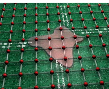
Researchers studying the behavior of nanoscale materials at the Department of Energy’s Oak Ridge National Laboratory have uncovered remarkable behavior that could advance microprocessors beyond today’s silicon-based chips.
The study, featured on the cover of Advanced Electronic Materials ("Chip Architectures: Multimodal Responses of Self-Organized Circuitry in Electronically Phase Separated Materials"), shows that a single crystal complex oxide material, when confined to micro- and nanoscales, can act like a multi-component electrical circuit. This behavior stems from an unusual feature of certain complex oxides called phase separation, in which tiny regions in the material exhibit vastly different electronic and magnetic properties.
It means individual nanoscale regions in complex oxide materials can behave as self-organized circuit elements, which could support new multifunctional types of computing architectures.
An study found that complex oxide materials can self-organize into electrical circuits, which creates the possibility for new types of computer chips
An ORNL study found that complex oxide materials can self-organize into electrical circuits, which creates the possibility for new types of computer chips.
“Within a single piece of material, there are coexisting pockets of different magnetic and/or electronic behaviors,” said ORNL’s Zac Ward, the study’s corresponding author. “What was interesting in this study was that we found we can use those phases to act like circuit elements. The fact that it is possible to also move these elements around offers the intriguing opportunity of creating rewritable circuitry in the material.”
Because the phases respond to both magnetic and electrical fields, the material can be controlled in multiple ways, which creates the possibility for new types of computer chips.
“It’s a new way of thinking about electronics, where you don’t just have electrical fields switching off and on for your bits,” Ward said. “This is not going for raw power. It’s looking to explore completely different approaches towards multifunctional architectures where integration of multiple outside stimuli can be done in a single material.”
As the computing industry looks to move past the limits of silicon-based chips, the ORNL proof-of-principle experiment shows that phase separated materials could be a way beyond the “one-chip-fits-all” approach. Unlike a chip that performs only one role, a multifunctional chip could handle several inputs and outputs that are tailored to the needs of a specific application.
“Typically you would need to link several different components together on a computer board if you wanted access to multiple outside senses,” Ward said. “One big difference in our work is that we show certain complex materials already have these components built in, which may cut down on size and power requirements.”
The researchers demonstrated their approach on a material called LPCMO, but Ward notes that other phase-separated materials have different properties that engineers could tap into.
“The new approach aims to increase performance by developing hardware around intended applications,” he said. “This means that materials and architectures driving supercomputers, desktops, and smart phones, which each have very different needs, would no longer be forced to follow a one-chip-fits-all approach.”
Share on:


Testimonial
"Advertising in PCB007 Magazine has been a great way to showcase our bare board testers to the right audience. The I-Connect007 team makes the process smooth and professional. We’re proud to be featured in such a trusted publication."
Klaus Koziol - atgSuggested Items
Curing and Verification in PCB Shadow Areas
09/17/2025 | Doug Katze, DymaxDesign engineers know a simple truth that often complicates electronics manufacturing: Light doesn’t go around corners. In densely populated PCBs, adhesives and coatings often fail to fully cure in shadowed regions created by tall ICs, connectors, relays, and tight housings.
Marcy’s Musings: Advancing the Advanced Materials Discussion
09/17/2025 | Marcy LaRont -- Column: Marcy's MusingsAs the industry’s most trusted global source of original content about the electronics supply chain, we continually ask you about your concerns, what you care about, and what you most want to learn about. Your responses are insightful and valuable. Thank you for caring enough to provide useful feedback and engage in dialogue.
September 2025 PCB007 Magazine: The Future of Advanced Materials
09/16/2025 | I-Connect007 Editorial TeamMoore’s Law is no more, and the advanced material solutions being developed to grapple with this reality are surprising, stunning, and perhaps a bit daunting. Buckle up for a dive into advanced materials and a glimpse into the next chapters of electronics manufacturing.
I-Connect007 Launches Advanced Electronics Packaging Digest
09/15/2025 | I-Connect007I-Connect007 is pleased to announce the launch of Advanced Electronics Packaging Digest (AEPD), a new monthly digital newsletter dedicated to one of the most critical and rapidly evolving areas of electronics manufacturing: advanced packaging at the interconnect level.
Panasonic Industry will Double the Production Capacity of MEGTRON Multi-layer Circuit Board Materials Over the Next Five Years
09/15/2025 | Panasonic Industry Co., Ltd.Panasonic Industry Co., Ltd., a Panasonic Group company, announced plans for a major expansion of its global production capacity for MEGTRON multi-layer circuit board materials today. The company plans to double its production over the next five years to meet growing demand in the AI server and ICT infrastructure markets.