


 The Marketing Minute: Cracking the Code of Technical Marketing
 Trouble in Your Tank: Implementing Direct Metallization in Advanced Substrate Packaging


Deep Insight Into Interfaces
September 19, 2016 | Universität WürzburgEstimated reading time: 4 minutes
Interfaces between different materials and their properties are of key importance for modern technology. Together with an international team, physicists of Würzburg University have developed a new method, which allows them to have an extremely precise glance at these interfaces and to model their properties.
In his Nobel Lecture on December 8, 2000, Herbert Kroemer coined the saying “the interface is the device”. Kroemer referred to the mature field of semiconductor heterostructures, which form the basis of all modern electronics.
However, now, in the advent of novel, powerful devices based on the more complex and versatile topological and correlated materials, the statement is timelier than ever. Such materials are at the focus of research in the Department of Physics and Astronomy at Würzburg University: Currently, 16 groups are working in this field, and a Collaborative Research Center (CRC 1170) was established in 2015, which is funded by the German Science Foundation (DFG) with nearly 10 Million euro.
Publication in Nature Quantum Materials
In the recent years physicists from Würzburg University and coworkers from Germany, Canada, the U.S.A. and Korea developed a new method to uncover important charge properties of correlated oxide interfaces with unprecedented atomic scale resolution. The team of Professor Vladimir Hinkov and his coworkers report about this experimental method in the current issue of the Nature Journal “NPJ Quantum Materials”.
“Conventional electronic chips are based on networks of so-called p-n junctions, interfaces between semiconductors carrying positive and negative charges, respectively,” says Vladimir Hinkov, describing the background of this research. There are several drawbacks to such a setup: First, the junctions are thick, often of the order of hundreds of interatomic spacings. Second, operating the network requires the movement of many electrons, which costs a lot of energy due to electrical resistance. Third, semiconductors do not intrinsically have magnetic properties and their electron configuration is very basic. “This dramatically limits the ways to build functional junctions and to realize magnetic applications,” Hinkov reports.
Versatile properties require sophisticated methods
Transition-metal oxides, on the other hand, exhibit many different properties: Some of them are ferromagnetic, others are antiferromagnetic, and others in turn are high-temperature superconductors with very unconventional properties. Forming interfaces between such materials yields a plethora of phenomena, which hold promise for novel applications such as different sensors, lossless computer memory and ultrafast processors. The price one has to pay is that more sophisticated tools are necessary to study them: This is due to the variety of phenomena and due to the much shorter length scale, over which the properties of oxides change at such heterointerfaces, which is often just a few atomic spacings.
Of crucial importance is the behavior of electrons at the interface: Do they tend to accumulate? Which orbitals do they occupy, i.e. how do the electron clouds arrange around the atoms? Is there magnetic order, i.e. do the tiny magnetic moments of the electrons called spins align relative to each other, establishing magnetic order? Physicists around the world are seeking for answers to these questions.
Measurements on an atomic scale
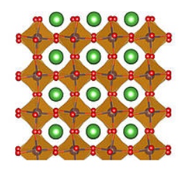
Hinkov and coworkers developed a new method and analysis software, and it provides answers. It is based on “resonant x-ray reflectometry”, a technique exploiting x-ray light created at a synchrotron, with the atomic-scale resolution of less than one nanometer. The physicists apply the technique on thin films of lanthanum cobalt oxide, a material that has interesting magnetic properties.
In their present work, however, the scientists have concentrated on another aspect: "Before we can delve in the rich magnetic phenomena of this material, we first have to solve a fundamental, very wide spread problem," says Professor Hinkov. "Like many other materials, such as simple table salt and many semiconductors, lanthanum cobalt oxide consists of charged particles. These so-called ions form a sequence of positively and negatively charged atomic layers, stacked to a 15 nanometer thin film. “One can show that enormous electrostatic fields form between the layers, which is a problem, since they cost a lot of energy,” as Vladimir Hinkov explains.
“Nature is economical and avoids these field energy costs: It brings positive and negative charges to the opposite faces of the film, respectively, just like between the plates of a capacitor. A new field is formed, which is opposite to the original one and which cancels it."
Corrugated interfaces constitute a problem
This accumulation of pure electronic charge at the film faces is called “electronic reconstruction”. According to the physicists, this is a very elegant solution, since it preserves the film face smoothness. For materials, in which electronic reconstruction is not possible, the compensating charge is provided by comparatively large ions, which results in corrugated film faces. As Hinkov explains, such corrugations are detrimental for devices based on film interfaces, especially when, like in transition-metal oxides, the material properties change on an atomic scale at the interface.
Exploiting the new method, the present work shows microscopic evidence that electronic reconstruction is indeed realized at transition-metal oxide interfaces. The method also provides a possibility to study the microscopic properties of such interfaces, which are not limited to electronic reconstruction, but encompass the arrangement of chemical elements, the electronic occupation of atomic orbitals and the spin orientation.
Successful by close, international collaboration
The special “Würzburg environment” and the close international collaboration enabled this successful work. "Such a scientific endeavor is only possible when experts from many different fields work closely together," says Professor Hinkov. One needs excellent samples, high-precision x-ray scattering instruments, which are operated at modern synchrotron light sources, a dedicated software, and last but not least “colleagues who are willing to spend day and night at the synchrotron to perform the measurements."
Share on:


Testimonial
"We’re proud to call I-Connect007 a trusted partner. Their innovative approach and industry insight made our podcast collaboration a success by connecting us with the right audience and delivering real results."
Julia McCaffrey - NCAB GroupSuggested Items
Curing and Verification in PCB Shadow Areas
09/17/2025 | Doug Katze, DymaxDesign engineers know a simple truth that often complicates electronics manufacturing: Light doesn’t go around corners. In densely populated PCBs, adhesives and coatings often fail to fully cure in shadowed regions created by tall ICs, connectors, relays, and tight housings.
Marcy’s Musings: Advancing the Advanced Materials Discussion
09/17/2025 | Marcy LaRont -- Column: Marcy's MusingsAs the industry’s most trusted global source of original content about the electronics supply chain, we continually ask you about your concerns, what you care about, and what you most want to learn about. Your responses are insightful and valuable. Thank you for caring enough to provide useful feedback and engage in dialogue.
September 2025 PCB007 Magazine: The Future of Advanced Materials
09/16/2025 | I-Connect007 Editorial TeamMoore’s Law is no more, and the advanced material solutions being developed to grapple with this reality are surprising, stunning, and perhaps a bit daunting. Buckle up for a dive into advanced materials and a glimpse into the next chapters of electronics manufacturing.
I-Connect007 Launches Advanced Electronics Packaging Digest
09/15/2025 | I-Connect007I-Connect007 is pleased to announce the launch of Advanced Electronics Packaging Digest (AEPD), a new monthly digital newsletter dedicated to one of the most critical and rapidly evolving areas of electronics manufacturing: advanced packaging at the interconnect level.
Panasonic Industry will Double the Production Capacity of MEGTRON Multi-layer Circuit Board Materials Over the Next Five Years
09/15/2025 | Panasonic Industry Co., Ltd.Panasonic Industry Co., Ltd., a Panasonic Group company, announced plans for a major expansion of its global production capacity for MEGTRON multi-layer circuit board materials today. The company plans to double its production over the next five years to meet growing demand in the AI server and ICT infrastructure markets.