


 The Marketing Minute: Cracking the Code of Technical Marketing
 Trouble in Your Tank: Implementing Direct Metallization in Advanced Substrate Packaging


Nanoscale Tetrapods Could Provide Early Warning of a Material’s Failure
September 20, 2016 | LBLEstimated reading time: 3 minutes
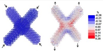
Light-emitting, four-armed nanocrystals could someday form the basis of an early warning system in structural materials by revealing microscopic cracks that portend failure, thanks to recent research by scientists from the U.S. Department of Energy’s Lawrence Berkeley National Laboratory (Berkeley Lab) and UC Berkeley.
The researchers embedded tetrapod-shaped quantum dots, which are nanosized semiconducting particles, in a polymer film. The tetrapods’ cores emit fluorescent light when their arms are twisted or bent out of shape. This indicates the polymer is undergoing a degree of tensile or compressive strain, from which stress over sub-micron-scale regions of the material can be detected. Such stress can cause nanoscale cracks to develop into macroscopic failure. Initial tests show the tetrapods can cycle more than 20 times without losing their ability to sense stress, and they don’t degrade the strength of the polymer in which they’re matrixed.
So far the scientists have tested their approach in the lab, but in practice, all that would be needed to detect the tetrapods’ fluorescent warning is an off-the-shelf, portable spectrometer. A person could point a spectrometer at a steel beam, airplane wing, or any material that has the tetrapods embedded inside, and the spectrometer could potentially detect incipient cracks that are only 100 nanometers long.
“This is the length scale at which cracks develop, which is when you want to catch them, well before the material fails,” says Shilpa Raja, who conducted the research while she was an affiliate in Berkeley Lab’s Materials Sciences Division and a PhD student at UC Berkeley. Raja is now a postdoctoral scholar at Stanford University. Robert Ritchie and Paul Alivisatos, also of the Materials Sciences Division and UC Berkeley, are the co-corresponding authors of a paper on this research published online in the journal Nano Letters (2016, vol. 16, issue 8, pgs. 5060-5067).
“Our approach could also be a big step toward self-healing smart materials. The tetrapods could be coupled with nanosized repair particles to form a material that senses local stress and then repairs itself,” adds Raja.
In addition to materials applications, the tetrapods could potentially be used to detect the presence of cancerous cells in tissue samples because cancerous cells have different mechanical properties than healthy cells, such as an increased stiffness.
To develop the technique, the scientists started with a polymer widely used in airframes and other structures. They mixed tetrapod nanocrystals into the polymer and cast slabs of the mixture in petri dishes. The slabs were then mounted in a tensile tester and exposed to a laser. This allowed the researchers to simultaneously measure the slab’s fluorescence and mechanical stress.
“This is a low-cost fabrication technique, and it resulted in the best optomechanical agreement between fluorescence and mechanical tests sensed by a nanocrystal in a film,” says Raja.
Raja says the tetrapods’ shape makes them very sensitive to stress. Their four arms act as antennae that take stress from their immediate environment, amplify the stress, and transfer it to the core. The color of light emitted by the core indicates the degree of stress (and strain) felt by the arms.
Their approach promises to be a big improvement over current ways to detect nanoscale stress in materials, particularly in the field. This can be done in the lab with techniques like atomic force microscopy and nano-indentation techniques, but these require a very controlled environment. Over the past five years, scientists have developed ways to matrix other stress-sensing nanoparticles into materials, but these methods have a very low signal-to-noise ratio and don’t use visible light detection. In addition, some of these approaches degrade the mechanical properties of the material they’re embedded in, or they can’t cycle back and forth, meaning they can only give a warning signal once.
Atom-scale computer simulations of the tetrapod were conducted at the National Energy Research Scientific Computing Center (NERSC). And electron tomography of the tetrapods under stress was conducted at the Molecular Foundry. Both facilities are DOE Office of Science User Facilities located at Berkeley Lab.
The research was funded in part by the Department of Energy’s Office of Science.
Share on:


Testimonial
"Our marketing partnership with I-Connect007 is already delivering. Just a day after our press release went live, we received a direct inquiry about our updated products!"
Rachael Temple - AlltematedSuggested Items
Curing and Verification in PCB Shadow Areas
09/17/2025 | Doug Katze, DymaxDesign engineers know a simple truth that often complicates electronics manufacturing: Light doesn’t go around corners. In densely populated PCBs, adhesives and coatings often fail to fully cure in shadowed regions created by tall ICs, connectors, relays, and tight housings.
Marcy’s Musings: Advancing the Advanced Materials Discussion
09/17/2025 | Marcy LaRont -- Column: Marcy's MusingsAs the industry’s most trusted global source of original content about the electronics supply chain, we continually ask you about your concerns, what you care about, and what you most want to learn about. Your responses are insightful and valuable. Thank you for caring enough to provide useful feedback and engage in dialogue.
September 2025 PCB007 Magazine: The Future of Advanced Materials
09/16/2025 | I-Connect007 Editorial TeamMoore’s Law is no more, and the advanced material solutions being developed to grapple with this reality are surprising, stunning, and perhaps a bit daunting. Buckle up for a dive into advanced materials and a glimpse into the next chapters of electronics manufacturing.
I-Connect007 Launches Advanced Electronics Packaging Digest
09/15/2025 | I-Connect007I-Connect007 is pleased to announce the launch of Advanced Electronics Packaging Digest (AEPD), a new monthly digital newsletter dedicated to one of the most critical and rapidly evolving areas of electronics manufacturing: advanced packaging at the interconnect level.
Panasonic Industry will Double the Production Capacity of MEGTRON Multi-layer Circuit Board Materials Over the Next Five Years
09/15/2025 | Panasonic Industry Co., Ltd.Panasonic Industry Co., Ltd., a Panasonic Group company, announced plans for a major expansion of its global production capacity for MEGTRON multi-layer circuit board materials today. The company plans to double its production over the next five years to meet growing demand in the AI server and ICT infrastructure markets.