


 Driving Innovation: Mechanical and Optical Processes During Rigid-flex Production
 It’s Only Common Sense: Your Biggest Competitor Is Complacency
 The Chemical Connection: Onshoring PCB Production—Daunting but Certainly Possible


SelectConnect Technologies Publishes White Paper on Laser Direct Structuring
April 5, 2017 | SelectConnect TechnologiesEstimated reading time: 1 minute
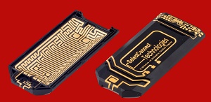
SelectConnect Technologies has published the white paper, “Trace Width and Space Limitations for Laser Direct Structuring.” The white paper details a study that was conducted to determine how close laser direct structuring (LDS) traces can be created and metallized without inducing over plating or bridging on PET/PBT material.
A geometric pattern with varying trace widths and spacing distances were structured onto plaques made from the three different materials. The plaques were subsequently plated with copper, nickel, and immersion gold and examined for signs of over plating. Trace widths and spacing were measured using video microscopy equipment.
Laser direct structuring (LDS) is the first step of a manufacturing process that creates circuit traces on three-dimensional molded thermoplastic components. Currently the leading technology for producing cell phone antennas, LDS has also been widely employed to manufacture a range of components for use in medical devices, security shields, automotive sensors, and GPS antennas-- anywhere product miniaturization requires embedding circuits onto a molded component of a device.
About SelectConnect Technologies
SelectConnect Technologies specializes in the production of three-dimensional molded interconnect devices (3D-MID), offering both laser direct structuring (LDS) and 2-shot injection capabilities. Working with LPKF since 2010, the company has produced thousands of laser direct structured components for a wide range of applications. With expertise in electroless metallization, SelectConnect also produces molded interconnect device plating to construct circuitry with the comparable function and performance of a printed circuit board.
To read and download the white paper, please click here or email solutions@selectconnettech.com.
Share on:


Testimonial
"In a year when every marketing dollar mattered, I chose to keep I-Connect007 in our 2025 plan. Their commitment to high-quality, insightful content aligns with Koh Young’s values and helps readers navigate a changing industry. "
Brent Fischthal - Koh YoungSuggested Items
Episode 6 of Ultra HDI Podcast Series Explores Copper-filled Microvias in Advanced PCB Design and Fabrication
10/15/2025 | I-Connect007I-Connect007 has released Episode 6 of its acclaimed On the Line with... American Standard Circuits: Ultra High Density Interconnect (UHDI) podcast series. In this episode, “Copper Filling of Vias,” host Nolan Johnson once again welcomes John Johnson, Director of Quality and Advanced Technology at American Standard Circuits, for a deep dive into the pros and cons of copper plating microvias—from both the fabricator’s and designer’s perspectives.
Nolan’s Notes: Tariffs, Technologies, and Optimization
10/01/2025 | Nolan Johnson -- Column: Nolan's NotesLast month, SMT007 Magazine spotlighted India, and boy, did we pick a good time to do so. Tariff and trade news involving India was breaking like a storm surge. The U.S. tariffs shifted India from one of the most favorable trade agreements to the least favorable. Electronics continue to be exempt for the time being, but lest you think that we’re free and clear because we manufacture electronics, steel and aluminum are specifically called out at the 50% tariff levels.
MacDermid Alpha & Graphic PLC Lead UK’s First Horizontal Electroless Copper Installation
09/30/2025 | MacDermid Alpha & Graphic PLCMacDermid Alpha Electronics Solutions, a leading supplier of integrated materials and chemistries to the electronics industry, is proud to support Graphic PLC, a Somacis company, with the installation of the first horizontal electroless copper metallization process in the UK.
Electrodeposited Copper Foils Market to Grow by $11.7 Billion Over 2025-2032
09/18/2025 | Globe NewswireThe global electrodeposited copper foils market is poised for dynamic growth, driven by the rising adoption in advanced electronics and renewable energy storage solutions.
MacDermid Alpha Showcases Advanced Interconnect Solutions at PCIM Asia 2025
09/18/2025 | MacDermid Alpha Electronics SolutionsMacDermid Alpha Electronic Solutions, a global leader in materials for power electronics and semiconductor assembly, will showcase its latest interconnect innovations in electronic interconnect materials at PCIM Asia 2025, held from September 24 to 26 at the Shanghai New International Expo Centre, Booth N5-E30