


 Dan’s Biz Bookshelf: 'A View from the Top: Moving from Success to Significance'
 The Chemical Connection: The Practice of Doing Business in Foreign Lands
 It’s Only Common Sense: Pricing PCBs? It’s All in Their Heads


Erasable Ink for 3D Printing
May 2, 2017 | KITEstimated reading time: 2 minutes
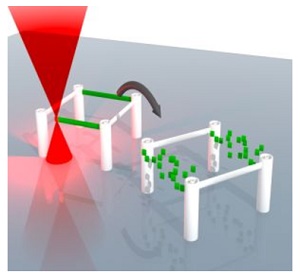
3D printing by direct laser writing produces micrometer-sized structures with precisely defined properties. Researchers of Karlsruhe Institute of Technology (KIT) have now developed a method to erase the ink used for 3D printing. In this way, the small structures of up to 100 nm in size can be erased and rewritten repeatedly. One nanometer corresponds to one millionth of a millimeter. This development opens up many new applications of 3D fabrication in biology or materials sciences, for instance.
Direct laser writing means that a computer-controlled, focused laser beam generates the structure in a photoresist similar to a pen. “Developing an ink that can be erased again was one of the big challenges in direct laser writing,” Professor Christopher Barner-Kowollik of KIT’s Institute for Chemical Technology and Polymer Chemistry says. The scientists have now met with success: They have developed an ink with reversible bonding, the building blocks of which can be separated from each other. The printed structure is simply erased by immersing it into a chemical solvent. At the point of erasure, a new structure can be written. In this way, the structure can be modified repeatedly.
The process was developed in close cooperation with the group of Professor Martin Wegener at the Institute of Applied Physics and the Institute of Nanotechnology of KIT. The physicists developed highly specialized 3D printers that produce scaffolds of up to 100 nm in size by direct laser writing.
“The ink with defined breaking points can be used for a variety of applications,” doctoral student and first author Markus Zieger says. Structures written with erasable ink can be integrated into structures made of non-erasable ink: Support constructions can be produced by 3D printing, which are similar to those used when building bridges and removed later on. It is also possible to further develop 3D designer petri dishes for use in biology. Recently, such structures were designed by KIT to grow cell cultures in three dimensions on the laboratory scale. “During cell growth, parts of the 3D microscaffold could be removed again to study how the cells react to the changed environment,” Martin Wegener explains. According to the scientists, it is also feasible to produce reversible wire bonds from erasable conducting structures in the future. A permanent ink can be mixed with a non-permanent ink to influence the properties of the printed material and make it more or less porous, for instance.
The new process is presented in the renowned journal Angewandte Chemie under the heading “Cleaving Direct Laser Written Microstructures on Demand.” The reviewers rated this publication a “very important paper.” 3D printing already is indispensable in many fabrication areas. Its importance is increasing. “According to estimations, some 10 percent of all goods will be produced by 3D printing in 2030,” Barner-Kowollik and Wegener say.
Markus M. Zieger, Patrick Mueller, Alexander S. Quick, Martin Wegener, Christopher Barner-Kowollik: Cleaving Direct Laser Written Microstructures on Demand. Angewandte Chemie 2017, 129, 1-6; DOI: 10.1002/anie.201701593
About Karlsruhe Institute of Technology (KIT)
Karlsruhe Institute of Technology (KIT) pools its three core tasks of research, higher education, and innovation in a mission. With about 9,300 employees and 25,000 students, KIT is one of the big institutions of research and higher education in natural sciences and engineering in Europe.
Share on:


Testimonial
"We’re proud to call I-Connect007 a trusted partner. Their innovative approach and industry insight made our podcast collaboration a success by connecting us with the right audience and delivering real results."
Julia McCaffrey - NCAB GroupSuggested Items
TI DLP® Technology Delivers High-Precision Digital Lithography for Advanced Packaging
10/02/2025 | Texas InstrumentsTexas Instruments is enhancing the next generation of digital lithography with the introduction of the DLP991UUV digital micromirror device (DMD), the company’s highest resolution direct imaging solution to date.
Rigetti, in Collaboration with QphoX, Awarded $5.8M AFRL Contract to Advance Superconducting Quantum Networking
09/29/2025 | RigettiRigetti Computing, Inc., a pioneer in hybrid quantum-classical computing, announced that it was awarded a three-year, $5.8 million contract from the Air Force Research Laboratory (AFRL) to advance superconducting quantum networking.
High-Tech Hill Technology Park Opens: Four New Factories Launched
09/26/2025 | TeltonikaThe ambitious vision announced in late 2020 to build a world-class technology park in Liepkalnis, Vilnius, has become a reality. AGP Investments, led by entrepreneur Arvydas Paukštys, together with high-tech leaders Teltonika and TLT, today inaugurated four new factories at the Vilnius High-Tech Hill Technology Park.
LPKF to Unveil CuttingMaster 2240 Cx at Productronica
09/26/2025 | LPKF Laser & ElectronicsLPKF Laser & Electronics SE will be showcasing the CuttingMaster 2240 Cx as part of the Fraunhofer IZM production line at this year's Productronica in Munich, demonstrating state-of-the-art laser technology in action.
Signal Integrity: A Game of Margins
09/25/2025 | Andy Shaughnessy, Design007 MagazineAs the founder of Wild River Technology, Al Neves deals with some of the most challenging aspects of signal integrity. Wild River’s engineers consult with high-tech companies that work at very high speeds and frequencies, often above 100G. Al is always a fun interview, so we asked him to share his thoughts on the current state of signal integrity engineering.