


 Driving Innovation: Mechanical and Optical Processes During Rigid-flex Production
 It’s Only Common Sense: Your Biggest Competitor Is Complacency
 The Chemical Connection: Onshoring PCB Production—Daunting but Certainly Possible


Floating Fields for Fine Fabrication
May 18, 2017 | A*STAREstimated reading time: 2 minutes
Magnetic levitation (Maglev) is well known for its use in high-speed rail networks, but could also be applied at smaller scales in medicine and electronics. To do so, researchers must be able to precisely control electromagnetic fields so that they can move and rotate objects without touching them.
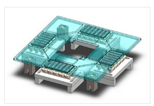
The levitating platform developed by Teo and co-workers contains arrays of permanent magnets floating above several coils of wire. The movement of the platform is controlled by varying the current in the coils.
Now, Teo Tat Joo and co-workers at the A*STAR Singapore Institute of Manufacturing Technology (SIMTech) and National University of Singapore have developed a Maglev system that can produce linear and rotational motion in all three dimensions1. This system provides nanometer-scale precision in these movements, and is simpler and potentially less energy-intensive than other recent attempts.
“Today’s existing precision mechatronics systems can only be classified as having one micrometer positioning accuracy over one meter — one part-per-million or 1 PPM,” says Teo. “On the other hand, Maglev technology has the potential to achieve a truly nanometer positioning system — 0.001 PPM.”
To build their new Maglev system, Teo and co-workers employed a special arrangement of permanent magnets called a Halbach array, which produces a strong magnetic field on one side but not the other. They positioned four Halbach arrays on a square platform above several energized coils of wire (see image), and used analytical force modeling to work out how the magnets and coils would interact. Then, by carefully controlling the electrical current in different coils, they were able to move or rotate the square platform at several different speeds (see video), with a positional error of just 50 nanometers.
The video demonstrates precisely-controlled linear and circular motion of the levitating platform at various speeds.
“One of the main technical challenges we faced was that the large number of coils, with high electrical resistance, require a high power supply,” says Teo. “We are currently developing a scheme that allows selective switching of the coils; this will improve the energy efficiency and significantly reduce the cost of the Maglev system.”
Perhaps the most promising uses of the Maglev system developed by the A*STAR team would be in processes that require a particle-free or vacuum environment, as Teo explains: “The contactless nature of Maglev ensures that no contaminating particles are generated from friction between surfaces. For example, future wafer lithography processes such as extreme UV lithography, which operates in a vacuum, will require a Maglev system to handle the wafer.”
Teo also suggests that Maglev technology could replace conventional conveyor belts in factories. Unlike traditional conveyors that can only move objects on pre-defined tracks, Maglev could move several objects simultaneously to different desired locations.
Share on:


Testimonial
"Our marketing partnership with I-Connect007 is already delivering. Just a day after our press release went live, we received a direct inquiry about our updated products!"
Rachael Temple - AlltematedSuggested Items
OSI Systems Reports Fiscal Q1 2026 Financial Results
10/31/2025 | BUSINESS WIREOSI Systems, Inc. announced its financial results for the first quarter of fiscal 2026.
Aircraft Wire and Cable Market to surpass USD 3.2 Billion by 2034
10/30/2025 | Global Market Insights Inc.The global aircraft wire and cable market was valued at USD 1.8 billion in 2024 and is estimated to grow at a CAGR of 5.9% to reach USD 3.2 billion by 2034, according to recent report by Global Market Insights Inc.
David Schild Addresses Printed Circuit Board Issues as a Panelist at AUVSI
10/30/2025 | PCBAAOn October 28, Printed Circuit Board Association of America executive director David Schild appeared on a panel at the Association for Uncrewed Vehicle Systems International (AUVSI) conference on the topic of “First Supply Chains: Strengthening the Industrial Base for Autonomy.” PCBAA sponsored the event and Schild shared his views on issues facing the American microelectronics industry.
Real Time with... SMTAI 2025: Koh Young's Innovations in SMT Inspection Technology
10/30/2025 | Real Time with...SMTAIJoel Scutchfield discusses his background as well as Koh Young's advancements in inspection technology. The conversation covers various inspection systems, including the flagship Zenith 2 system and recent software upgrades.
BAE Contract Agreed with the Republic of Türkiye for Typhoon Aircraft
10/28/2025 | BAE SystemsThe UK Government has announced a c.£5.4 billion agreement with the Republic of Türkiye for the purchase of 20 Typhoon aircraft and an associated weapons and integration package, sustaining more than 20,000 highly skilled jobs across the UK supply chain.