


 Dan’s Biz Bookshelf: Four Important Books You Need to Read (Not Just Say You Have)
 The Marketing Minute: Cracking the Code of Technical Marketing


Large Single-Crystal Graphene Could Advance Scalable 2D Materials
March 23, 2018 | Oak Ridge National LaboratoryEstimated reading time: 4 minutes
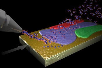
A new method to produce large, monolayer single-crystal-like graphene films more than a foot long relies on harnessing a “survival of the fittest” competition among crystals. The novel technique, developed by a team led by the Department of Energy’s Oak Ridge National Laboratory, may open new opportunities for growing the high-quality two-dimensional materials necessary for long-awaited practical applications.
Image caption: In a controlled environment, the fastest-growing orientation of graphene crystals overwhelms the others and gets "evolutionarily selected" into a single crystal, even on a polycrystalline substrate, without having to match the substrate’s orientation. An Oak Ridge National Laboratory-led team developed the novel method that produces large, monolayer single-crystal-like graphene films more than a foot long. Credit: Andy Sproles/Oak Ridge National Laboratory, U.S. Dept. of Energy
Making thin layers of graphene and other 2D materials on a scale required for research purposes is common, but they must be manufactured on a much larger scale to be useful.
Graphene is touted for its potential of unprecedented strength and high electrical conductivity and can be made through well-known approaches: separating flakes of graphite—the silvery soft material found in pencils—into one-atom-thick layers, or growing it atom by atom on a catalyst from a gaseous precursor until ultrathin layers are formed.
The ORNL-led research team used the latter method—known as chemical vapor deposition, or CVD—but with a twist. In a study published in Nature Materials, they explained how localized control of the CVD process allows evolutionary, or self-selecting, growth under optimal conditions, yielding a large, single-crystal-like sheet of graphene.
“Large single crystals are more mechanically robust and may have higher conductivity,” ORNL lead coauthor Ivan Vlassiouk said. “This is because weaknesses arising from interconnections between individual domains in polycrystalline graphene are eliminated.”
“Our method could be the key not only to improving large-scale production of single-crystal graphene but to other 2D materials as well, which is necessary for their large-scale applications,” he added.
Much like traditional CVD approaches to produce graphene, the researchers sprayed a gaseous mixture of hydrocarbon precursor molecules onto a metallic, polycrystalline foil. However, they carefully controlled the local deposition of the hydrocarbon molecules, bringing them directly to the edge of the emerging graphene film. As the substrate moved underneath, the carbon atoms continuously assembled as a single crystal of graphene up to a foot in length.
“The unencumbered single-crystal-like graphene growth can go almost continuously, as a roll-to-roll and beyond the foot-long samples demonstrated here,” said Sergei Smirnov, coauthor and New Mexico State University professor.
As the hydrocarbons touch down the hot catalyst foil, they form clusters of carbon atoms that grow over time into larger domains until coalescing to cover the whole substrate. The team previously found that at sufficiently high temperatures, the carbon atoms of graphene did not correlate, or mirror, the substrate’s atoms, allowing for nonepitaxial crystalline growth.
Since the concentration of the gas mixture strongly influences how quickly the single crystal grows, supplying the hydrocarbon precursor near the existing edge of single graphene crystal can promote its growth more effectively than the formation of new clusters.
“In such a controlled environment, the fastest-growing orientation of graphene crystals overwhelms the others and gets ‘evolutionarily selected’ into a single crystal, even on a polycrystalline substrate, without having to match the substrate’s orientation, which usually happens with standard epitaxial growth,” Smirnov said.
They found that to ensure optimal growth, it was necessary to create a “wind” that helps to eliminate the cluster formations. “It was imperative that we create an environment where the formation of new clusters ahead of the growth front was totally suppressed, and enlargement of just the growing edge of the large graphene crystal was not hindered,” Vlassiouk said. “Then, and only then, nothing stands in the way of the ‘fittest’ crystalline growth when the substrate is moving.”
The team’s theoreticians, led by coauthor Rice University professor Boris Yakobson, provided a model explaining which crystal orientations possess the unique properties that make them fittest in the run for survival, and why the choice of a winner may depend on the substrate and the precursors.
“If graphene or any 2D material ever advances to industrial scale, this approach will be pivotal, similar to Czochralski’s method for silicon.” Yakobson said. “Manufacturers can rest assured that when a large, wafer-size raw layer is cut for any device fabrication, each resulting piece will be a quality monocrystal. This potentially huge, impactful role motivates us to explore theoretical principles to be as clear as possible.”
Practical scaling up of graphene using the team’s method remains to be seen, but the researchers believe their evolutionary selection single-crystal growth method could also be applied to promising alternative 2D materials such as boron nitride, also known as “white graphene,” and molybdenum disulfide.
The team’s paper, “Evolutionary selection growth of two-dimensional materials on polycrystalline substrates,” included coauthors Ivan Vlassiouk, Yijing Stehle, Raymond R. Unocic, Arthur P. Baddorf, Ilia N. Ivanov, Nickolay V. Lavrik and Frederick List of Oak Ridge National Laboratory; Philip D. Rack of ORNL and University of Tennessee; Pushpa Raj Pudasini of UT; Nitant Gupta, Ksenia Bets and Boris I. Yakobson of Rice University; and Sergei Smirnov of New Mexico State University.
The research was supported by ORNL’s Laboratory Directed Research and Development program, ORNL’s technology transfer royalty funded Technology Innovation Program, and DOE’s Advanced Research Projects Agency-Energy. Microscopy work was supported as part of the Fluid Interface Reactions, Structures and Transport Center, an Energy Frontier Research Center. This work also leveraged ORNL’s Center for Nanophase Materials Sciences, a DOE Office of Science User Facility.
ORNL is managed by UT-Battelle for DOE’s Office of Science. The Office of Science is the single largest supporter of basic research in the physical sciences in the United States, and is working to address some of the most pressing challenges of our time. For more information, please click here.
Share on:


Testimonial
"The I-Connect007 team is outstanding—kind, responsive, and a true marketing partner. Their design team created fresh, eye-catching ads, and their editorial support polished our content to let our brand shine. Thank you all! "
Sweeney Ng - CEE PCBSuggested Items
Curing and Verification in PCB Shadow Areas
09/17/2025 | Doug Katze, DymaxDesign engineers know a simple truth that often complicates electronics manufacturing: Light doesn’t go around corners. In densely populated PCBs, adhesives and coatings often fail to fully cure in shadowed regions created by tall ICs, connectors, relays, and tight housings.
Marcy’s Musings: Advancing the Advanced Materials Discussion
09/17/2025 | Marcy LaRont -- Column: Marcy's MusingsAs the industry’s most trusted global source of original content about the electronics supply chain, we continually ask you about your concerns, what you care about, and what you most want to learn about. Your responses are insightful and valuable. Thank you for caring enough to provide useful feedback and engage in dialogue.
September 2025 PCB007 Magazine: The Future of Advanced Materials
09/16/2025 | I-Connect007 Editorial TeamMoore’s Law is no more, and the advanced material solutions being developed to grapple with this reality are surprising, stunning, and perhaps a bit daunting. Buckle up for a dive into advanced materials and a glimpse into the next chapters of electronics manufacturing.
I-Connect007 Launches Advanced Electronics Packaging Digest
09/15/2025 | I-Connect007I-Connect007 is pleased to announce the launch of Advanced Electronics Packaging Digest (AEPD), a new monthly digital newsletter dedicated to one of the most critical and rapidly evolving areas of electronics manufacturing: advanced packaging at the interconnect level.
Panasonic Industry will Double the Production Capacity of MEGTRON Multi-layer Circuit Board Materials Over the Next Five Years
09/15/2025 | Panasonic Industry Co., Ltd.Panasonic Industry Co., Ltd., a Panasonic Group company, announced plans for a major expansion of its global production capacity for MEGTRON multi-layer circuit board materials today. The company plans to double its production over the next five years to meet growing demand in the AI server and ICT infrastructure markets.