


 The Marketing Minute: AI Is Watching Your Marketing Habits
 Trouble in Your Tank: The Role of Organic Solderability Preservatives in Advanced Packaging
 It’s Only Common Sense: Lighten Up!


The special properties of ‘topological materials’ typically occur at their surface. These materials, for example insulators that do conduct current at their surface, are expected to play a major role in future quantum computers. Scientists of the University of Twente and the University of Amsterdam now demonstrate a new property: the non-superconducting material bismuth shows lossless current conduction. What's even more special: it doesn’t just occur at the surface but in the inside, the bulk, of the material as well. The scientists publish their findings in Nature Materials of October. In a special review on this paper, the results are called ‘truly desired and inspiring’.
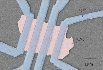
Image Caption: By applying superconducting electrodes, made of niobium, to a thin crystal flake of bismuth doped with antimony, a superconducting current flows through the material at a temperature of 10 milli Kelvin. In a superconductor, paired electrons, so-called Cooper pairs, are responsible for conduction. This is not the mechanism inside the bismuth: here, Majorana particles are responsible.
Topological materials have gained more and more interest, especially after Thouless, Haldane and Kosterlitz won the Nobel Prize in Physics for it, in 2016. New terms like topotronics and spintronics were even introduced. The materials get their particular properties by playing with the order of energy levels. By ‘twisting’ these levels, a material that doesn’t conduct any current under normal circumstances, will suddenly become a conductor, but at its surface exclusively. Not only the transport of electrons is involved, but their spin as well – this describes the way the electron turns around its own axis and its magnetical properties.
Superconductivity
In their Nature Materials paper, the researchers now demonstrate a that the transport and spin of electrons are related, in a topological material. Thanks to this property, a non-superconducting material will even be able to conduct current without resistance. Majorana ‘quasi particles’ play a major role in this. What makes it even more special: this is not a property that can only be observed at the surface. Measurements show that superconduction also takes place inside the material, in the ‘bulk’. This is very interesting, as it makes the properties less vulnerable to, for example, noise or pollution.
The material that is used for this, bismuth with a little antimony, keeps surprising. Over the years, it has turned into a ‘model material’ for electronic properties. In bismuth, the number of electrons available for conduction is so low that it can hardly be called a metal. But the electrons in this ‘semimetal’ do move like particles at the speed of light.
Beyond 2D
For future electronics and quantum computing, 2D materials like graphene seem candidates. The newly discovered property show that this doesn’t have to be a limiting factor: 3D building blocks might be possible as well, just like in current-day silicon-based electronic devices.
The research has been done by the 'Quantum Transport in Matter' group, part of University of Twente’s MESA+ Institute. The UT scientists closely collaborated with colleagues of the Van der Waals – Zeeman Institute of the University of Amsterdsam.
The research is an excellent example of the UT research theme Shaping our world with smart materials.
The paper ‘4π periodic Andreev bound states in a Dirac Semimetal’, by Chuan Li, Jorrit de Boer, Bob de Ronde, Shyama Ramankutty, Erik van Heumen, Yingkai Huang, Anne de Visser, Alexander Golubov, Mark Golden and Alexander Brinkman is in the October print issue of ‘Nature Materials’.


