


 Flexible Thinking: Designing Flex Circuits for Dynamic Reliability
 Global PCB Connections: Rigid-flex and Flexible PCBs—The Backbone of Modern Electronics
 Happy’s Tech Talk #29: Bend-to-Install Semi-flex FR-4


As the sun set on a glorious February day, which could easily have been moved from spring to give us a foretaste that better weather was on its way, the Institute of Circuit Technology hosted its first 2019 seminar at the Woodland Grange Hotel in Royal Leamington Spa in the Midlands of England on February 26.
The diverse programme of four presentations was introduced by ICT Chairman Andy Cobley, a professor at Coventry University, who stood in for Bill Wilkie, who had been taken ill at short notice.
Cobley thanked Wilkie for his hard work in organising the seminar. He also noted that Pete Starkey was recovering from a recent accident and wished him a speedy recovery.
First Presentation
The first presentation was “Bioleaching of Metals from PCBs” by Dr. Mahsa Baniasadi of Coventry University. The project had been supported by Innovate U.K. and had an industrial partner. She highlighted the potential for metal recovery from electronic waste (WEEE), given that there were around 44.7 metric tonnes of WEEE produced annually around the world. Then, Dr. Baniasadi showed a comparison of the metal contents of PCBs and ores to demonstrate the potential for recovering metals from such waste.
Dr. Baniasadi also described the conventionally-used pyro- and hydro-metallurgical recovery methods, but more sustainable approaches were needed. Bioleaching was one such method that relies on the production of acids and ligands via the use of micro-organisms. She further detailed the mechanisms employed; for example, biocyanidisation could be used for gold recovery, using cyanogenic bacteria to produce the requisite cyanide. Moreover, the microorganisms could be used to degrade the cyanide subsequently. Also, Dr. Baniasadi showed the chemical reaction of the complex metal cyanide formation reaction and made comparisons between biocyanidation and chemical cyanidation approaches. The bio process had a lower cost and a life cycle assessment had been undertaken.
Further, non-metal content removal was an essential prerequisite for metal recovery; it could include the use of a shaking table and electrostatic separation. Dr. Baniasadi also presented data for base metal recovery and reviewed the effect of operational parameters. Key factors impacting the recovery efficiency included glycine concentration, pH, pulp density, dissolved oxygen levels, and particle size. Finally, she explained a commercial metal extraction approach known as the Merrill-Crowe process that used activated carbon, ion exchange, and electrowinning.
Second Presentation
Jonathan Swanston, Soluboard development lead at Jiva Materials, gave the second presentation titled “Soluboard®: A New Composite for Electronics.” Jiva Materials is just over one year old and aims to redefine the way printed circuits are made with a particular emphasis on a fully recyclable PCB laminate that could replace FR-4. Swanston detailed problems with end-of-life PCBs, and their traditional methods of treatment, including the release of toxins into the environment.
Jiva Materials’ new product, Soluboard, was based on the use of a natural fibre-reinforced composite and a soluble polymer that dissolved in hot water. The product is flame retarded using phosphorus-based materials, which are fully biodegradable and non-toxic. Swanston described the potential market for the product in the context of the overall substrate market and the current focus on supplying to EU instrumentation makers, where there is a lot of interest. The current price is around £20.00 per square metre, and the aim is also to supply the product to domestic appliance manufacturers. Jiva Materials is currently working with Printed Electronics Limited (PEL) and Loughborough University, and proof of concept had been demonstrated. The key properties are favourable compared to those of FR-4.
Third Presentation
The third presentation was “Developing Universal Solutions to Automotive Materials Challenges” by Alun Morgan, technology ambassador at Ventec International Group. Morgan had very kindly stepped in at the last minute to replace the scheduled speaker, Emma Hudson, who had unexpectedly been called away on a business trip. He began by outlining the automotive application hot spots requiring thermal management, and described LED lighting and its advantages, such as lower power consumption and long lifetime. Morgan also outlined Haitz’s law, how the cost per lumen fell by a factor of 10 per decade, and how the amount of light generated per package increased by a factor of 20 for a given wavelength.
Next, Morgan introduced basic thermodynamics and detailed the principles of the first, second, third, and “zeroth” laws. He also described principles of heat transfer and convection, conduction, and radiation in the context of LED thermal management. LEDs are more efficient than incandescent lamps, but almost 75% of the input electrical power is turned to heat. The conventional methods of managing the heat from LEDs included the use of heatsinks, but Morgan noted other important methods, including the use of thermally conductive PCBs with enhanced thermal properties compared to FR-4.
Morgan further listed the thermal conductivities of a range of well-known materials and equations relating to convective and radiative heat transfer along with an example calculation model for thermal radiation. He illustrated the importance of being able to survive thermal cycling (e.g., in a headlamp unit) through the use of two case studies where failure had occurred. Failure analysis showed that the CTE mismatch between various materials used in the construction had been the likely cause. The problem was resolved by using materials with more closely matched CTEs and by optimising moduli. Morgan further illustrated future requirements by referencing published industry roadmaps.
Final Presentation
Ian Mayoh, technical support manager EMEA of Ventec Europe Ltd., gave the final presentation of the evening entitled “Back to Basics.” He began by detailing PCB base materials and the various types of resins systems and why they were used. Mayoh then discussed the range of glasses and other reinforcements (e.g., D glass and NE glass both found use in low-loss and high-speed applications). Next, he used a schematic to show the production process stages for base materials and explained brominated flame retardants and alternative organo-phosphorus materials and their functional mechanisms. In recent years, there has been a move away from the use of dicyandiamide curing agents to the phenolic-based systems, which were needed to provide compatibility with the higher temperatures encountered with lead-free soldering.
Mayoh also presented data showing the differences in laminate thermal expansion below and above the glass transition temperature (Tg) and explained techniques for measuring Tg such as differential scanning calorimetry (DSC) and thermo-mechanical analysis (TMA). He discussed dielectric properties of the various materials used in making a laminate and reviewed the effects of dielectric constant on board design and signal integrity. Copper foil profile was another increasingly critical consideration, particularly for boards working at higher frequencies where the skin effect meant conduction was only in the outer few microns of the copper. Similar to Morgan, Mayoh concluded his presentation by referencing future substrate trends as recorded in the latest industry roadmaps.
Many Thanks
Steve Payne closed the meeting and invited members of the ICT to participate more by considering submitting papers to the ICT journal or by joining the ICT Council. He asked the audience to thank the four speakers for their excellent presentations. Finally, Steve asked the attendees to thank Ventec International Group for their kind sponsorship of the seminar, and the response was a loud round of applause.
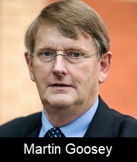
Technical editor’s note: I most gratefully acknowledge the efforts of Professor Martin Goosey in preparing this review and Alun Morgan for providing the photographs. Many thanks! —Pete Starkey


