


 American Made Advocacy: Smart Policies Can Ensure AI Data Centers Are Secure
 Beyond the Board: Early Engagement Means Faster Prototyping for Defense Programs
 Defense Speak Interpreted: The Autonomous Plane Battle—Skyborg Vs. Loyal Wingman


DARPA Seeks to Make Scalable On-Chip Security Pervasive
March 31, 2019 | DARPAEstimated reading time: 4 minutes
For the past decade, cybersecurity threats have moved from high in the software stack to progressively lower levels of the computational hierarchy, working their way towards the underlying hardware. The rise of the Internet of Things (IoT) has driven the creation of a rapidly growing number of accessible devices and a multitude of complex chip designs needed to enable them.
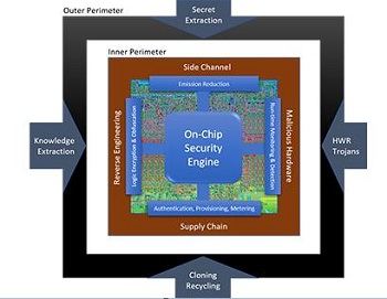
Image Caption: The image depicts the approach expected under the AISS program. The defenses under AISS will focus on securing the inner perimeter from four specific attack surfaces that are most relevant to digital ASICs and SoCs. These include side channel attacks, reverse engineering attacks, supply chain attacks, and malicious hardware attacks. The on-chip security engine AISS seeks to develop will aid designers in assessing which defense mechanisms are most appropriate based on the potential attack surface and the likelihood of a compromise.
With this rapid growth comes increased opportunity for economic and nation-state adversaries alike to shift their attention to chips that enable complex capabilities across commercial and defense applications. The consequences of a hardware cyberattack are significant as a compromise could potentially impact not millions, but billions of devices.
Despite growing recognition of the issue, there are no common tools, methods, or solutions for chip-level security currently in wide use. This is largely driven by the economic hurdles and technical trade-offs often associated with secure chip design. Incorporating security into chips is a manual, expensive, and cumbersome task that requires significant time and a level of expertise that is not readily available in most chip and system companies. The inclusion of security also often requires certain trade-offs with the typical design objectives, such as size, performance, and power dissipation. Further, modern chip design methods are unforgiving – once a chip is designed, adding security after the fact or making changes to address newly discovered threats is nearly impossible.
“Today, it can take six to nine months to design a modern chip, and twice as long if you want to make that same design secure,” said Serge Leef, a program manager in DARPA’s Microsystems Technology Office (MTO). “While large merchant semiconductor companies are investing in in-house personnel to manually incorporate security into their high-volume silicon, mid-size chip companies, system houses, and start-ups with small design teams who create lower volume chips lack the resources and economic drivers to support the necessary investment in scalable security mechanisms, leaving a majority of today’s chips largely unprotected.”
To ease the burden of developing secure chips, DARPA developed the Automatic Implementation of Secure Silicon (AISS) program. AISS aims to automate the process of incorporating scalable defense mechanisms into chip designs, while allowing designers to explore economics versus security trade-offs and maximize design productivity. The objective of the program is to develop a design tool and IP ecosystem – which includes tool vendors, chip developers, IP licensers, and the open source community – that will allow security to be inexpensively incorporated into chip designs with minimal effort and expertise, ultimately making scalable on-chip security pervasive.
Leef continued, “The security, design, and economic objectives of a chip can vary based on its intended application. As an example, a chip design with extreme security requirements may have to accept certain tradeoffs. Achieving the required security level may cause the chip to become larger, consume more power, or deliver slower performance. Depending on the application, some or all of these tradeoffs may be acceptable, but with today’s manual processes it’s hard to determine where tradeoffs can be made.”
AISS seeks to create a novel, automated chip design flow that will allow the security mechanisms to scale consistently with the goals of the design. The design flow will provide a means of rapidly evaluating architectural alternatives that best address the required design and security metrics, as well as varying cost models to optimize the economics versus security tradeoff. The target AISS system – or system on chip (SoC) – will be automatically generated, integrated, and optimized to meet the objectives of the application and security intent. These systems will consist of two partitions – an application specific processor partition and a security partition implementing the on-chip security features. This approach is novel in that most systems today do not include a security partition due to its design complexity and cost of integration. By bringing greater automation to the chip design process, the burden of security inclusion can be profoundly decreased.
While the threat landscape is ever evolving and expansive, AISS seeks to address four specific attack surfaces that are most relevant to digital ASICs and SoCs. These include side channel attacks, reverse engineering attacks, supply chain attacks, and malicious hardware attacks. “Strategies for resisting threats vary widely in cost, complexity, and invasiveness. As such, AISS will help designers assess which defense mechanisms are most appropriate based on the potential attack surface and the likelihood of a compromise,” said Leef.
In addition to incorporating scalable defense mechanisms, AISS seeks to ensure that the IP blocks that make up the chip remain secure throughout the design process and are not compromised as they move through the ecosystem. As such, the program will also aim to move forward provenance and integrity validation techniques for preexisting design components by advancing current methods or inventing novel technical approaches. These techniques may include IP watermarking and threat detection to help validate the chip’s integrity and IP provenance throughout its lifetime.
AISS is part of the second phase of DARPA’s Electronics Resurgence Initiative (ERI) – a five-year, upwards of $1.5 billion investment in the future of domestic, U.S. government, and defense electronics systems. Under ERI Phase II, DARPA is exploring the development of trusted electronics components, including the advancement of electronics that can enforce security and privacy protections. AISS will help address this mission through its efforts to enable scalable on-chip security.
Share on:


Testimonial
"Our marketing partnership with I-Connect007 is already delivering. Just a day after our press release went live, we received a direct inquiry about our updated products!"
Rachael Temple - AlltematedSuggested Items
NEDME 2025 Draws Strong Northwest Crowd, Builds on Tradition of Regional Collaboration
10/31/2025 | NEDMEThe NW Electronics Design & Manufacturing Expo (NEDME) 2025 once again brought together the Pacific Northwest community for a full day of learning, networking, and industry connections.
Keysight Advances Quantum Engineering with New System-Level Simulation Solution
10/30/2025 | BUSINESS WIREKeysight Technologies, Inc. announced the release of Quantum System Analysis, a breakthrough Electronic Design Automation (EDA) solution that enables quantum engineers to simulate and optimize quantum systems at the system level.
WestDev Announces Advanced Thermal Analysis Integration for Pulsonix PCB Design Suite
10/29/2025 | WestDev Ltd.Pulsonix, the industry-leading PCB design software from WestDev Ltd., announced a major enhancement to its design ecosystem: a direct interface between Pulsonix and ADAM Research's TRM (Thermal Risk Management) analysis software.
Industry Veteran Dr. Helen Song Joins Celera Semiconductor to Lead Product Design
10/28/2025 | PRNewswireCelera Semiconductor, the analog industry leader using AI to automate the entire product development flow, today announced that Dr. Helen Song has joined the company as vice president of Product Design.
Mapping the EV Landscape: Markets, Platforms, and Powertrains
10/28/2025 | Stanton Rak, SF Rak Companye-Mobility is the defining transformation of 21st-century transportation. As legacy OEMs, startups, and governments race to electrify vehicle fleets, the landscape of e-Mobility is expanding into previously unimaginable territory. But with innovation comes complexity, and with complexity, a need for systems that are not only high-performing but also reliably engineered for the long haul. Understanding the diversity and scale of the EV marketplace is essential to grasping the reliability challenges ahead.