


 The Marketing Minute: Cracking the Code of Technical Marketing
 Trouble in Your Tank: Implementing Direct Metallization in Advanced Substrate Packaging


Lasers Enable Engineers to Weld Ceramics, No Furnace Required
August 26, 2019 | UC San DiegoEstimated reading time: 2 minutes
Smartphones that don’t scratch or shatter. Metal-free pacemakers. Electronics for space and other harsh environments. These could all be made possible thanks to a new ceramic welding technology developed by a team of engineers led by the University of California San Diego.
The process uses an ultrafast pulsed laser to melt ceramic materials along the interface and fuse them together. It works in ambient conditions and uses less than 50 watts of laser power, making it more practical than current ceramic welding methods that require heating the parts in a furnace.
Ceramics have been fundamentally challenging to weld together because they need extremely high temperatures to melt, exposing them to extreme temperature gradients that cause cracking, explained senior author Javier E. Garay, a professor of mechanical engineering and materials science and engineering at UC San Diego, who led the work in collaboration with UC Riverside professor and chair of mechanical engineering Guillermo Aguilar. Ceramic materials are of great interest because they are biocompatible, extremely hard and shatter resistant, making them ideal for biomedical implants and protective casings for electronics. However, current ceramic welding procedures are not conducive to making such devices.
“Right now there is no way to encase or seal electronic components inside ceramics because you would have to put the entire assembly in a furnace, which would end up burning the electronics,” Garay said.
Garay, Aguilar and colleagues’ solution was to aim a series of short laser pulses along the interface between two ceramic parts so that heat builds up only at the interface and causes localized melting. They call their method ultrafast pulsed laser welding.
To make it work, the researchers had to optimize two aspects: the laser parameters (exposure time, number of laser pulses, and duration of pulses) and the transparency of the ceramic material. With the right combination, the laser energy couples strongly to the ceramic, allowing welds to be made using low laser power (less than 50 watts) at room temperature. “The sweet spot of ultrafast pulses was two picoseconds at the high repetition rate of one megahertz, along with a moderate total number of pulses. This maximized the melt diameter, minimized material ablation, and timed cooling just right for the best weld possible,” Aguilar said.
“By focusing the energy right where we want it, we avoid setting up temperature gradients throughout the ceramic, so we can encase temperature-sensitive materials without damaging them,” Garay said.
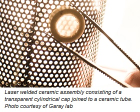
As a proof of concept, the researchers welded a transparent cylindrical cap to the inside of a ceramic tube. Tests showed that the welds are strong enough to hold vacuum.
“The vacuum tests we used on our welds are the same tests that are used in industry to validate seals on electronic and optoelectronic devices,” said first author Elias Penilla, who worked on the project as a postdoctoral researcher in Garay’s research group at UC San Diego.
The process has so far only been used to weld small ceramic parts that are less than two centimeters in size. Future plans will involve optimizing the method for larger scales, as well as for different types of materials and geometries.
Share on:


Testimonial
"The I-Connect007 team is outstanding—kind, responsive, and a true marketing partner. Their design team created fresh, eye-catching ads, and their editorial support polished our content to let our brand shine. Thank you all! "
Sweeney Ng - CEE PCBSuggested Items
Curing and Verification in PCB Shadow Areas
09/17/2025 | Doug Katze, DymaxDesign engineers know a simple truth that often complicates electronics manufacturing: Light doesn’t go around corners. In densely populated PCBs, adhesives and coatings often fail to fully cure in shadowed regions created by tall ICs, connectors, relays, and tight housings.
Marcy’s Musings: Advancing the Advanced Materials Discussion
09/17/2025 | Marcy LaRont -- Column: Marcy's MusingsAs the industry’s most trusted global source of original content about the electronics supply chain, we continually ask you about your concerns, what you care about, and what you most want to learn about. Your responses are insightful and valuable. Thank you for caring enough to provide useful feedback and engage in dialogue.
September 2025 PCB007 Magazine: The Future of Advanced Materials
09/16/2025 | I-Connect007 Editorial TeamMoore’s Law is no more, and the advanced material solutions being developed to grapple with this reality are surprising, stunning, and perhaps a bit daunting. Buckle up for a dive into advanced materials and a glimpse into the next chapters of electronics manufacturing.
I-Connect007 Launches Advanced Electronics Packaging Digest
09/15/2025 | I-Connect007I-Connect007 is pleased to announce the launch of Advanced Electronics Packaging Digest (AEPD), a new monthly digital newsletter dedicated to one of the most critical and rapidly evolving areas of electronics manufacturing: advanced packaging at the interconnect level.
Panasonic Industry will Double the Production Capacity of MEGTRON Multi-layer Circuit Board Materials Over the Next Five Years
09/15/2025 | Panasonic Industry Co., Ltd.Panasonic Industry Co., Ltd., a Panasonic Group company, announced plans for a major expansion of its global production capacity for MEGTRON multi-layer circuit board materials today. The company plans to double its production over the next five years to meet growing demand in the AI server and ICT infrastructure markets.