


 Global PCB Connections: Rigid-flex and Flexible PCBs—The Backbone of Modern Electronics
 Flexible Thinking: The Key to a Successful Flex Circuit Design Transfer
 Happy’s Tech Talk #29: Bend-to-Install Semi-flex FR-4


Decreasing Bend Radius and Improving Reliability—Part I
October 11, 2019 | Kelsey Smith, All FlexEstimated reading time: 1 minute
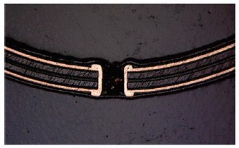
Application: Design guidelines to improve the flexibility and reliability of flexible circuits.
Many of the issues that arise when using a flex circuit come from a lack of knowledge about how to properly design one, especially when the circuit is required to bend. Many novices will design a circuit that calls for bending the flex in too tight of a bend radius, which can cause damage to the circuit and lower the reliability of the end product. This series of articles will focus on the seven key aspects to consider when designing for maximum durability and maximum “flexibility.” It is important to know that because flexibility is a relative term, this study will instead use the phrase "reducing bend radius." Here are two of the seven design strategies (please see Part II and Part III for more tips):
1. Reduce overall thickness:
IPC guidelines typically list minimum bend radius of 6X the circuit thickness for single-sided flex, 10X for double-sided flex, and 20X for multiple layer flex. The area of focus is the thickness where flexing or bending will occur, which should be only in a location with conductors and not plated through-holes. Thickness can best be reduced by:
A. Using thinner copper
B. Using adhesive-less base materials
C. Stagger conductors
D. Specifying button plating or pads only plating
Any flex circuit with plated through-holes will need to be either panel plated or button plated. Button plating is preferred because it only plates the vias and leaves the conductors un-plated and which does not increase the thickness.
2. Use only rolled annealed (RA) copper:
There are two common types of copper; rolled annealed (RA) and electro-deposited (ED) copper.
A. Rolled annealed copper is best for achieving a tighter bend radius.
B. It is also important for you to put on your drawings the direction of the grain in relation to where the tight bending will occur.
Go to Part two of this article.
Share on:


Testimonial
"Your magazines are a great platform for people to exchange knowledge. Thank you for the work that you do."
Simon Khesin - Schmoll MaschinenSuggested Items
The Impact of the AI Boom on PCB and Raw Materials Supply Chains
11/13/2025 | Mark Goodwin, Ventec International GroupThe PCB industry is entering a period of unprecedented structural change, driven by the demands of artificial intelligence and advanced computing. What was once a cyclical market has become a capacity race. It’s one that rewards foresight, collaboration, and strategic supply partnerships. Understanding these dynamics is essential for maintaining stability and growth across all market segments. This report, created by Ventec International Group, provides a clear view of how AI-driven demand is reshaping the PCB materials landscape and what actions are required to secure long-term supply.
Elementary, Mr. Watson: The Four Horsemen of Copper Confusion
11/12/2025 | John Watson -- Column: Elementary, Mr. WatsonIf there were a PCB Design Dictionary of Confusing Terms, the cover would feature four words that have baffled generations of engineers: polygons, pours, planes, and floods—or what I refer to as the four horsemen of copper confusion. They sound simple, as if they belong in a geometry textbook or a weather report, but in PCB design, they overlap, develop, and sound interchangeable until you realize they aren't.
Alpha Insights, Performance by Design: Understanding Heat at the Core of Every Design
11/11/2025 | Team Alpha -- Column: Alpha Insights: Performance by DesignPower isn’t just about current. It’s about control. As electronic systems grow smaller and faster, every amp and every layer generates a new source of heat. That heat is more than a byproduct. It’s a measure of efficiency, a benchmark of performance, and often the first indication of failure.
The Shaughnessy Report: Zee Plane! Zee Plane!
11/11/2025 | Andy Shaughnessy -- Column: The Shaughnessy ReportPlanes aren’t magic, but they are big time-savers. Without planes, designers would have to create thousands of traces to accomplish the same objectives. You can imagine the first time a designer thought about using a sheet of copper, asking, “Hey, why am I killing myself laying out all these traces? Can’t I just use this sheet of copper instead?”
November 2025 Design007 Magazine: Proper Plane Design
11/10/2025 | I-Connect007 Editorial TeamWithout planes, designers would have to create thousands of traces to accomplish the same objectives. Power planes provide low impedance and stable power to every component on the board, much like a large power bus. Ground planes stabilize reference voltage, improve thermal performance, and help preclude EMI issues. Power and ground plane design is often a battle of tradeoffs.