


 The Marketing Minute: Marketing With Layers
 The Right Approach: Electro-Tek—A Williams Family Legacy, Part 1
 It’s Only Common Sense: If You’re Not Differentiated, You’re Dead


PNC Inc. Invests in Limata’s X100 Laser Direct Imager
November 1, 2019 | PNC Inc.Estimated reading time: 2 minutes
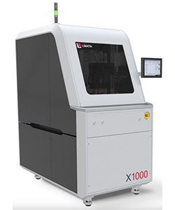
PNC Inc. recently purchased a LIMTA X1000 Laser Direct Imager from Limata, GmbH. With this purchase, all inner layers, outer layers, solder-mask and silkscreen are 100% digitally imaged, using two LDI systems.
In keeping with their commitment to continuous improvement, “This latest high precision technology is the first step of upgrading our LPI and screening departments in the coming weeks.” Said President Sam Sangani, “PNC INC chooses a LIMATA X1000 system solution (powered by LUVIR®) for their solder mask/silk screen process at its US Nutley, NJ site.”
Sangani continued, “LIMATA´s X1000 system solution powered by LUVIR technology® fully convinced our engineering team during the evaluation and production phase. We evaluated all available solutions for the solder mask and silk screen processes and we determined that LIMATA is by far, the most economical and the fastest machine with unmatched imaging quality in our industry. The capacity, flexibility and cost/performance ratio of the X1000 LUVIR DI system is outstanding in the market and offers PNC the ability to produce PCBs fully digital at significantly higher throughput levels by meeting all state-of-the art quality requirements for solder mask/Silk Screen imaging.” He added, “We recognize there is no cap on quality so pursuing it is an ongoing endeavor.”
The LIMATA X1000 series is a universal and cost-efficient Laser Direct Imaging (LDI) system platform designed for the flexible use in high-mix/ low-volume PCB manufacturing environments during the dry-film patterning or solder mask imaging process.
The new X1000 LDI system platform ensures maximum efficiency and throughput – i.e. from the use of LIMATA’s proprietary and in-house developed LUVIR (UV/IR) technology for solder mask imaging – at lowest possible TCO’s (Total Cost of Ownership) over the equipment life-cycle. Ideal for PCB manufacturers (or special PCB divisions of larger PCB makers) with high-mix/low-volume production mixes and imaging capacity/output requirements up to 500 panels per day (HDI, standard-rigid, flex) in a multi-shift operational mode.
About PNC Inc.
PNC Inc. is located in Nutley, NJ and is one of the country’s leading providers of rigid, rigid-flex and flex PCB’s and the largest of their kind in the region. After adopting the Total Concept philosophy, PNC is now able to provide customers with PCB design, fabrication and assembly solutions all under one roof. They are a one-stop shop for all things related to PC boards. They are continuously expanding their extensive list of state-of-the-art equipment while maintaining a focus on energy and cost efficiency in order to provide the best product at the best price possible.
Share on:


Testimonial
"We’re proud to call I-Connect007 a trusted partner. Their innovative approach and industry insight made our podcast collaboration a success by connecting us with the right audience and delivering real results."
Julia McCaffrey - NCAB GroupSuggested Items
Indium Experts to Deliver Technical Presentations at SMTA International
10/14/2025 | Indium CorporationAs one of the leading materials providers to the power electronics assembly industry, Indium Corporation experts will share their technical insight on a wide range of innovative solder solutions at SMTA International (SMTAI), to be held October 19-23 in Rosemont, Illinois.
Knocking Down the Bone Pile: Revamp Your Components with BGA Reballing
10/14/2025 | Nash Bell -- Column: Knocking Down the Bone PileBall grid array (BGA) components evolved from pin grid array (PGA) devices, carrying over many of the same electrical benefits while introducing a more compact and efficient interconnect format. Instead of discrete leads, BGAs rely on solder balls on the underside of the package to connect to the PCB. In some advanced designs, solder balls are on both the PCB and the BGA package. In stacked configurations, such as package-on-package (PoP), these solder balls also interconnect multiple packages, enabling higher functionality in a smaller footprint.
Indium to Showcase High-Reliability Solder and Flux-Cored Wire Solutions at SMTA International
10/09/2025 | Indium CorporationAs one of the leading materials providers in the electronics industry, Indium Corporation® will feature its innovative, high-reliability solder and flux-cored wire products at SMTA International (SMTAI), to be held October 19-23 in Rosemont, Illinois.
‘Create your Connections’ – Rehm at productronica 2025 in Munich
10/08/2025 | Rehm Thermal SystemsThe electronics industry is undergoing dynamic transformation: smart production lines, sustainability, artificial intelligence, and sensor technologies dominate current discussions.
Amplifying Innovation: New Podcast Series Spotlights Electronics Industry Leaders
10/08/2025 | I-Connect007In the debut episode, “Building Reliability: KOKI’s Approach to Solder Joint Challenges,” host Marcy LaRont speaks with Shantanu Joshi, Head of Customer Solutions and Operational Excellence at KOKI Solder America. They explore how advanced materials, such as crack-free fluxes and zero-flux-residue solder pastes, are addressing issues like voiding, heat dissipation, and solder joint reliability in demanding applications, where failure can result in costly repairs or even catastrophic loss.