


 Dan’s Biz Bookshelf: Four Important Books You Need to Read (Not Just Say You Have)
 The Marketing Minute: Cracking the Code of Technical Marketing


Researchers Discover a New Way to Control Infrared Light
January 31, 2020 | MITEstimated reading time: 5 minutes
In the 1950s, the field of electronics began to change when the transistor replaced vacuum tubes in computers. The change, which entailed replacing large and slow components with small and fast ones, was a catalyst for the enduring trend of miniaturization in computer design. No such revolution has yet hit the field of infrared optics, which remains reliant on bulky moving parts that preclude building small systems.
However, a team of researchers at MIT Lincoln Laboratory, together with Professor Juejun Hu and graduate students from MIT's Department of Materials Science and Engineering, is devising a way to control infrared light by using phase-change materials instead of moving parts. These materials have the ability to change their optical properties when energy is added to them.
“There are multiple possible ways where this material can enable new photonic devices that impact people’s lives,” says Hu. “For example, it can be useful for energy-efficient optical switches, which can improve network speed and reduce power consumption of internet data centers. It can enable reconfigurable meta-optical devices, such as compact, flat infrared zoom lenses without mechanical moving parts. It can also lead to new computing systems, which can make machine learning faster and more power-efficient compared to current solutions.”
A fundamental property of phase-change materials is that they can change how fast light travels through them (the refractive index). “There are already ways to modulate light using a refractive index change, but phase-change materials can change almost 1,000 times better,” says Jeffrey Chou, a team member formerly in the laboratory's Advanced Materials and Microsystems Group.
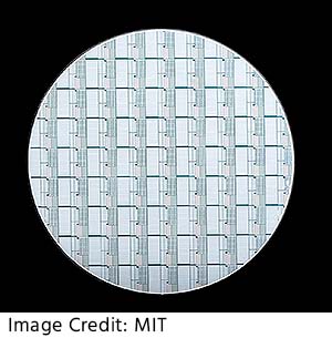
The team successfully controlled infrared light in multiple systems by using a new class of phase-change material containing the elements germanium, antimony, selenium, and tellurium, collectively known as GSST. This work is discussed in a paper published in Nature Communications.
A phase-change material's magic occurs in the chemical bonds that tie its atoms together. In one phase state, the material is crystalline, with its atoms arranged in an organized pattern. This state can be changed by applying a short, high-temperature spike of thermal energy to the material, causing the bonds in the crystal to break down and then reform in a more random, or amorphous, pattern. To change the material back to the crystalline state, a long- and medium-temperature pulse of thermal energy is applied.
“This changing of the chemical bonds allows for different optical properties to emerge, similar to the differences between coal (amorphous) and diamond (crystalline),” says Christopher Roberts, another Lincoln Laboratory member of the research team. “While both materials are mostly carbon, they have vastly different optical properties.”
Currently, phase-change materials are used for industry applications, such as Blu-ray technology and rewritable DVDs, because their properties are useful for storing and erasing a large amount of information. But so far, no one has used them in infrared optics because they tend to be transparent in one state and opaque in the other. (Think of the diamond, which light can pass through, and coal, which light cannot penetrate.) If light cannot pass through one of the states, then that light cannot be adequately controlled for a range of uses; instead, a system would only be able to work like an on/off switch, allowing light to either pass through the material or not pass through at all.
However, the research team found that that by adding the element selenium to the original material (called GST), the material's absorption of infrared light in the crystalline phase decreased dramatically — in essence, changing it from an opaque coal-like material to a more transparent diamond-like one. What's more, the large difference in the refractive index of the two states affects the propagation of light through them.
“This change in refractive index, without introducing optical loss, allows for the design of devices that control infrared light without the need for mechanical parts,” Roberts says.
As an example, imagine a laser beam that is pointing in one direction and needs to be changed to another. In current systems, a large mechanical gimbal would physically move a lens to steer the beam to another position. A thin-film lens made of GSST would be able change positions by electrically reprogramming the phase-change materials, enabling beam steering with no moving parts.
The team has already tested the material successfully in a moving lens. They have also demonstrated its use in infrared hyperspectral imaging, which is used to analyze images for hidden objects or information, and in a fast optical shutter that was able to close in nanoseconds.
The potential uses for GSST are vast, and an ultimate goal for the team is to design reconfigurable optical chips, lenses, and filters, which currently must be rebuilt from scratch each time a change is required. Once the team is ready to move the material beyond the research phase, it should be fairly easy to transition it into the commercial space. Because it's already compatible with standard microelectronic fabrication processes, GSST components could be made at a low cost and in large numbers.
Recently, the laboratory obtained a combinatorial sputtering chamber — a state-of-the-art machine that allows researchers to create custom materials out of individual elements. The team will use this chamber to further optimize the materials for improved reliability and switching speeds, as well as for low-power applications. They also plan to experiment with other materials that may prove useful in controlling visible light.
The next steps for the team are to look closely into real-world applications of GSST and understand what those systems need in terms of power, size, switching speed, and optical contrast.
“The impact [of this research] is twofold,” Hu says. "Phase-change materials offer a dramatically enhanced refractive index change compared to other physical effects — induced by electric field or temperature change, for instance — thereby enabling extremely compact reprogrammable optical devices and circuits. Our demonstration of bistate optical transparency in these materials is also significant in that we can now create high-performance infrared components with minimal optical loss.” The new material, Hu continues, is expected to open up an entirely new design space in the field of infrared optics.
This research was supported with funding from the laboratory's Technology Officeand the U.S. Defense Advanced Research Projects Agency.
Share on:


Testimonial
"Advertising in PCB007 Magazine has been a great way to showcase our bare board testers to the right audience. The I-Connect007 team makes the process smooth and professional. We’re proud to be featured in such a trusted publication."
Klaus Koziol - atgSuggested Items
Curing and Verification in PCB Shadow Areas
09/17/2025 | Doug Katze, DymaxDesign engineers know a simple truth that often complicates electronics manufacturing: Light doesn’t go around corners. In densely populated PCBs, adhesives and coatings often fail to fully cure in shadowed regions created by tall ICs, connectors, relays, and tight housings.
Marcy’s Musings: Advancing the Advanced Materials Discussion
09/17/2025 | Marcy LaRont -- Column: Marcy's MusingsAs the industry’s most trusted global source of original content about the electronics supply chain, we continually ask you about your concerns, what you care about, and what you most want to learn about. Your responses are insightful and valuable. Thank you for caring enough to provide useful feedback and engage in dialogue.
September 2025 PCB007 Magazine: The Future of Advanced Materials
09/16/2025 | I-Connect007 Editorial TeamMoore’s Law is no more, and the advanced material solutions being developed to grapple with this reality are surprising, stunning, and perhaps a bit daunting. Buckle up for a dive into advanced materials and a glimpse into the next chapters of electronics manufacturing.
I-Connect007 Launches Advanced Electronics Packaging Digest
09/15/2025 | I-Connect007I-Connect007 is pleased to announce the launch of Advanced Electronics Packaging Digest (AEPD), a new monthly digital newsletter dedicated to one of the most critical and rapidly evolving areas of electronics manufacturing: advanced packaging at the interconnect level.
Panasonic Industry will Double the Production Capacity of MEGTRON Multi-layer Circuit Board Materials Over the Next Five Years
09/15/2025 | Panasonic Industry Co., Ltd.Panasonic Industry Co., Ltd., a Panasonic Group company, announced plans for a major expansion of its global production capacity for MEGTRON multi-layer circuit board materials today. The company plans to double its production over the next five years to meet growing demand in the AI server and ICT infrastructure markets.