


 Dan’s Biz Bookshelf: Four Important Books You Need to Read (Not Just Say You Have)
 The Marketing Minute: Cracking the Code of Technical Marketing


Compound Photonics Backplane Enables World’s Smallest MicroLED AR Displays
May 5, 2020 | Business WireEstimated reading time: 2 minutes
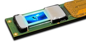
Compound Photonics US Corporation (CP), a global leader providing compact high-resolution microdisplay solutions for Augmented and Mixed Reality (AR/MR), announces today the wide availability of its high-performance digital backplane to leading microLED developers worldwide for integration into complete microdisplay subsystems.
CP re-engineered its market-ready LCoS backplane technology into an innovative constant current drive configuration for microLED pixels based on its industry-leading 0.26” diagonal (~3 ?m pixel) 1080p display format. microLED developers can accelerate their time to market by bonding their devices to a backplane driven by CP’s field-proven NOVA display drive architecture to enable complete display subsystems meeting critical AR requirements for compactness, optical performance and brightness with high frame rate, low latency and low power consumption.
“Our custom, constant current pixel circuit design provides greater tolerance to forward voltage variation and IR drops in the microLED array resulting in a previously unattainable level of uniformity. It additionally features globally on-the-fly programmable pixel current control that greatly increases the system bandwidth, enabling higher frame rates while maintaining full bit depth,” commented Ian Kyles, CP Vice President of Electrical/Software Engineering. “The backplane also has additional steering pixels beyond its native 2048x1080 resolution to enhance alignment/integration of the display within the optical system.”
MicroLED developers using this backplane can access CP’s monolithic integrated display module (IDM) (7.25 x 15.5 x 3.1 mm) with a low pin count interconnect and a direct MIPI input packaged into a compact subsystem amenable to smaller optical engine size. The IDM integrates CP’s proprietary NOVA drive architecture’s software defined platform to enable customizable frame-by-frame control of video frame rates (up to 240 Hz), bit depth, and other parameters to optimize for low latency, short persistence and low power while maintaining near 100% duty cycle according to type of image content and use case.
Andrew Shih, CP’s Marketing and Business Development Manager continued, “Process integration compatibility is also important, as bonding of the microLED array to the backplane requires a highly planar interface. CP’s backplane wafers feature excellent planarity, a direct benefit from extensive process tuning work to meet earlier LCoS requirements. By partnering with CP, whose backplane technology facilitates both wafer level process integration and a direct path to a complete NOVA-based microdisplay subsystem solution, microLED developers can focus on their core competencies in compound semiconductor photonic device engineering and process development while reducing development time and cost.”
A provisional backplane reference specification is presently available for customer review and CP is currently accepting engagements with leading microLED developers.
Share on:


Testimonial
"Our marketing partnership with I-Connect007 is already delivering. Just a day after our press release went live, we received a direct inquiry about our updated products!"
Rachael Temple - AlltematedSuggested Items
Alternative Manufacturing, Inc. (AMI) Announces Commitment to Excellence in Industrial, Defense, Aerospace, Renewables, and Robotics Markets
09/16/2025 | Alternative Manufacturing, Inc.Alternative Manufacturing, Inc. (AMI), a 100% employee-owned contract manufacturer, proudly reaffirms its leadership in the electronics manufacturing services (EMS) industry with a continued commitment to delivering high-quality PCBAs and box builds across the industrial, defense, aerospace, renewable energy, and robotics markets.
Sustainability and Selective Soldering
09/15/2025 | Dr. Samuel J. McMaster, Pillarhouse InternationalSustainability is more than just a buzzword for the electronics industry; it’s a key goal for all manufacturing processes. This is more than a box-ticking exercise or simply doing a small part for environmentally friendly processes. Moving toward sustainable solutions drives innovation and operational efficiency.
Trouble in Your Tank: Implementing Direct Metallization in Advanced Substrate Packaging
09/15/2025 | Michael Carano -- Column: Trouble in Your TankDirect metallization systems based on conductive graphite are gaining popularity throughout the world. The environmental and productivity gains achievable with this process are outstanding. Direct metallization reduces the costs of compliance, waste treatment, and legal issues related to chemical exposure. A graphite-based direct plate system has been devised to address these needs.
EV Group Achieves Breakthrough in Hybrid Bonding Overlay Control for Chiplet Integration
09/12/2025 | EV GroupEV Group (EVG), a leading provider of innovative process solutions and expertise serving leading-edge and future semiconductor designs and chip integration schemes, today unveiled the EVG®40 D2W—the first dedicated die-to-wafer overlay metrology platform to deliver 100 percent die overlay measurement on 300-mm wafers at high precision and speeds needed for production environments. With up to 15X higher throughput than EVG’s industry benchmark EVG®40 NT2 system designed for hybrid wafer bonding metrology, the new EVG40 D2W enables chipmakers to verify die placement accuracy and take rapid corrective action, improving process control and yield in high-volume manufacturing (HVM).
Integrating Uniplate PLBCu6 With the Digital Factory Suite
09/12/2025 | Giovanni Obino and Andreas Schatz, MKS' AtotechPrinted circuit board manufacturing is rapidly changing, driven by miniaturization, stringent reliability requirements, and growing pressure for sustainable production. Meeting these challenges requires more than incremental improvements; it demands a combination of precise equipment and real-time process intelligence. The pairing of Uniplate® PLBCu6 with the Digital Factory Suite (DFS) demonstrates how hardware and software can work together to create more responsive, resource-efficient manufacturing.