


 Driving Innovation: Mechanical and Optical Processes During Rigid-flex Production
 It’s Only Common Sense: Your Biggest Competitor Is Complacency
 The Chemical Connection: Onshoring PCB Production—Daunting but Certainly Possible


Compound Photonics Backplane Enables World’s Smallest MicroLED AR Displays
May 5, 2020 | Business WireEstimated reading time: 2 minutes
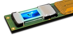
Compound Photonics US Corporation (CP), a global leader providing compact high-resolution microdisplay solutions for Augmented and Mixed Reality (AR/MR), announces today the wide availability of its high-performance digital backplane to leading microLED developers worldwide for integration into complete microdisplay subsystems.
CP re-engineered its market-ready LCoS backplane technology into an innovative constant current drive configuration for microLED pixels based on its industry-leading 0.26” diagonal (~3 ?m pixel) 1080p display format. microLED developers can accelerate their time to market by bonding their devices to a backplane driven by CP’s field-proven NOVA display drive architecture to enable complete display subsystems meeting critical AR requirements for compactness, optical performance and brightness with high frame rate, low latency and low power consumption.
“Our custom, constant current pixel circuit design provides greater tolerance to forward voltage variation and IR drops in the microLED array resulting in a previously unattainable level of uniformity. It additionally features globally on-the-fly programmable pixel current control that greatly increases the system bandwidth, enabling higher frame rates while maintaining full bit depth,” commented Ian Kyles, CP Vice President of Electrical/Software Engineering. “The backplane also has additional steering pixels beyond its native 2048x1080 resolution to enhance alignment/integration of the display within the optical system.”
MicroLED developers using this backplane can access CP’s monolithic integrated display module (IDM) (7.25 x 15.5 x 3.1 mm) with a low pin count interconnect and a direct MIPI input packaged into a compact subsystem amenable to smaller optical engine size. The IDM integrates CP’s proprietary NOVA drive architecture’s software defined platform to enable customizable frame-by-frame control of video frame rates (up to 240 Hz), bit depth, and other parameters to optimize for low latency, short persistence and low power while maintaining near 100% duty cycle according to type of image content and use case.
Andrew Shih, CP’s Marketing and Business Development Manager continued, “Process integration compatibility is also important, as bonding of the microLED array to the backplane requires a highly planar interface. CP’s backplane wafers feature excellent planarity, a direct benefit from extensive process tuning work to meet earlier LCoS requirements. By partnering with CP, whose backplane technology facilitates both wafer level process integration and a direct path to a complete NOVA-based microdisplay subsystem solution, microLED developers can focus on their core competencies in compound semiconductor photonic device engineering and process development while reducing development time and cost.”
A provisional backplane reference specification is presently available for customer review and CP is currently accepting engagements with leading microLED developers.
Share on:


Testimonial
"The I-Connect007 team is outstanding—kind, responsive, and a true marketing partner. Their design team created fresh, eye-catching ads, and their editorial support polished our content to let our brand shine. Thank you all! "
Sweeney Ng - CEE PCBSuggested Items
Unlocking the Promise of AI in Electronics Manufacturing
10/29/2025 | Shobhit Agrawal, Keysight TechnologiesThe electronics manufacturing industry is rapidly evolving as more complicated products are introduced in the production lines, which require technological advancements even in the production processes. The requirements for production that is efficient, product quality that is greater, and product life cycles that are shorter are more crucial than ever before. In the electronic device life cycle, from design to maintenance, test phases have a significant impact on the economy of the company. Test processes are closely linked to the production volume and impacted by the complexity of the product. For businesses to maintain their competitive edge, they need to adopt innovative solutions and redefine processes.
Driving Innovation: Mechanical and Optical Processes During Rigid-flex Production
10/28/2025 | Kurt Palmer -- Column: Driving InnovationRigid-flex printed circuit boards are a highly effective solution for placing complex circuitry in tight, three-dimensional spaces. They are now indispensable across a range of industries, from medical devices and aerospace to advanced consumer electronics, helping designers make the most efficient use of available space. However, their unique construction—combining rigid and flexible materials—presents a fundamental challenge for PCB manufacturers.
SMTAI 2025 Review: Reflecting on a Pragmatic and Forward-looking Industry
10/27/2025 | Marcy LaRont, I-Connect007Leaving the show floor on the final afternoon of SMTA International last week in Rosemont, Illinois, it was clear that the show remains a grounded, technically driven event that delivers a solid program, good networking, and an easy space to commune with industry colleagues and meet with customers.
The Marketing Minute: Marketing With Layers
10/15/2025 | Brittany Martin -- Column: The Marketing MinuteMarketing to a technical audience is like crafting a multilayer board: Each layer serves a purpose, from the surface story to the buried detail that keeps everything connected. At I-Connect007, we’ve learned that the best marketing campaigns aren’t built linearly; they’re layered. A campaign might start with a highly technical resource, such as an in-depth article, a white paper, or a podcast featuring an engineer delving into the details of a process. That’s the foundation, the substance that earns credibility.
Taking Control of PCB Verification One Step at a Time
10/09/2025 | Kirk Fabbri, Siemens EDAToday’s designs are as complex as ever, and engineers face tough decisions every day. Simulation and verification teams are confronted with a three-fold challenge: understanding the underlying theory, mastering the tools, and applying best practices.Engineers need to navigate a vast and ever-changing cast of design and simulation tools, often with overlapping functionality.