


 Dan’s Biz Bookshelf: ‘The Next RenAIssance: AI and the Expansion of Human Potential’
 The Chemical Connection: When the Industry Moves Faster Than the Standards
 Driving Innovation: Selecting the Right Laser Source


Rohm Reducing Size of Automotive Designs with Ultra-Compact MOSFETs
November 3, 2020 | Globe NewswireEstimated reading time: 2 minutes
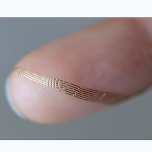
ROHM has released the ultra-compact AEC-Q101 qualified MOSFETs, RV8C010UN, RV8L002SN and BSS84X, best-in-class 1mm2 size that deliver automotive-grade reliability. The products are suitable for high-density applications such as ADAS and automotive ECUs.
The continuing electrification of vehicles in recent years has significantly increased the number of electronic and semiconductor components used per vehicle. Consequently, the need for a dramatic increase in component density has become even more important. For example, the average number of multilayer ceramic capacitors and semiconductor components installed in a single automotive ECU is expected to increase by 30%, from 186 in 2019 to 230 in 2025. At the same time, for high density automotive applications that demand greater miniaturization, studies are currently underway on bottom electrode packages that can achieve excellent heat dissipation in a compact form factor.
For automotive parts, automated optical inspection (AOI) is performed after mounting to ensure reliability, but with bottom electrode components the solder joint cannot be verified since the terminals are not visible, making it difficult to conduct visual inspection that meets automotive standards. ROHM has solved these issues with its original Wettable Flank technology that ensures an unprecedented side electrode height of 125?m in the 1.0mm × 1.0mm size and leading to increased adoption by a number of vehicle manufacturers.
Extremely high solder mounting reliability is achieved during AOI in automotive systems that require high quality. In addition, the new bottom electrode package simultaneously provides both breakthrough miniaturization and high heat dissipation (which are normally in a trade-off relationship), making it ideal for ADAS and automotive ECUs featuring higher board densities.
In addition to MOSFETs, ROHM is committed to continuing to expand its product lineup of bipolar transistors and diodes.
Key Features
1. Original Wettable Flank technology ensures a side electrode height of 125?m
With conventional bottom electrode packages, the sides of the lead frame cannot be plated, making it difficult to conduct AOI to verify the solder height required for automotive applications. In contrast, ROHM’s new MOSFETs leverage proprietary Wettable Flank technology to ensure a breakthrough side electrode height of 125?m in the 1.0mm × 1.0mm size. This enables stable toe fillet formation even with bottom electrode packages, allowing the solder condition to be verified by AOI after mounting.
2. Ultra-compact high heat dissipation MOSFETs support high density mounting
ROHM’s new MOSFETs achieve the same performance as 2.9mm × 2.4mm packages (SOT-23 packages) but in the smaller 1.0 × 1.0mm package (DFN1010 packages), reducing mounting area by approx. 85%. In addition, adopting a high heat dissipation bottom electrode structure improves heat dissipation (which normally decreases with size) by up to 65% over SOT-23. As a result, the RV8C010UN, RV8L002SN, and BSS84X are ideal for automotive ECUs and ADAS that are seeing higher board densities following increasing performance.
Share on:


Subscribe
Stay ahead of the technologies shaping the future of electronics with our latest newsletter, Advanced Electronics Packaging Digest. Get expert insights on advanced packaging, materials, and system-level innovation, delivered straight to your inbox.Subscribe now to stay informed, competitive, and connected.
Suggested Items
ACCM Unveils Negative and Near-zero CTE Materials for Large-Format AI Chips
04/21/2026 | Advanced Chip and Circuit MaterialsAdvanced Chip and Circuit Materials, Inc. (ACCM) has launched two new materials: Celeritas HM50, with a negative coefficient of thermal expansion (CTE) of -8 ppm/°C to offset the positive CTE and expansion of copper with temperature on circuit boards, and Celeritas HM001, with near-zero CTE and the low-loss performance needed for high-speed signal layers to 224 Gb/s and faster in artificial intelligence (AI) circuits.
SMTA Ultra HDI Symposium, Day 2: Fragile Supply Chains, Fierce Innovation
04/14/2026 | Marcy LaRont, I-Connect007The Arizona weather yielded another beautiful day as we gathered for the second day of SMTA’s annual UHDI symposium. After the first full day discussing the role of AI in business and the how-tos of implementation, Avondale Mayor Mike Pineda kicked off day two, proud to showcase his city and to declare its important place in the continued development of the West Valley, an increasingly important area for tech and manufacturing.
KYZEN Focuses on Aqueous and Stencil Cleaning Solutions at SMTA Monterrey Expo and Tech Forum
04/10/2026 | KYZEN'KYZEN, the global leader in innovative environmentally friendly cleaning chemistries, will exhibit at the SMTA Monterrey Expo & Tech Forum.
Solder Paste Innovations for Enhanced Reliability from MacDermid Alpha Electronics Solutions
04/10/2026 | Real Time with... APEX EXPOJason Fullerton of MacDermid Alpha Electronics Solutions discusses innovative alloys like Innolot MXE, low-temperature solder options, and polymer reinforcement strategies. Learn how these solutions address the growing demands of high-performance computing and larger component assemblies, ensuring optimal performance and cost-effectiveness.
Frank Sommer Discusses Selective Soldering Innovations for EVs
04/10/2026 | Real Time with... APEX EXPODan Beaulieu sits down with Frank Sommer, a selective soldering expert from Nordson Electronics Solutions, to discuss the resurgence of selective soldering driven by electric vehicle manufacturing, and the need for robust through-hole component integration. He also introduces Nordson's innovative SELECT Synchro selective soldering machine, designed for enhanced throughput and flexibility.