


 Global PCB Connections: Rigid-flex and Flexible PCBs—The Backbone of Modern Electronics
 Flexible Thinking: The Key to a Successful Flex Circuit Design Transfer
 Happy’s Tech Talk #29: Bend-to-Install Semi-flex FR-4


A New Platform for Controlled Design of Printed Electronics with 2D Materials
December 22, 2021 | Imperial College LondonEstimated reading time: 3 minutes
A study, published in Nature Electronics, led by Imperial College London and Politecnico di Torino researchers reveals the physical mechanisms responsible for the transport of electricity in printed two-dimensional (2D) materials.
The work identifies what properties of 2D material films need to be tweaked to make electronic devices to order, allowing rational design of a new class of high-performance printed and flexible electronics.
Silicon chips are the components that power most of our electronics, from fitness trackers to smartphones. However, their rigid nature limits their use in flexible electronics. Made of single-atom-thick layers, 2D materials can be dispersed in solution and formulated into printable inks, producing ultra-thin films that are extremely flexible, semi-transparent and with novel electronic properties.
This opens up the possibility of new types of devices, such as those that can be integrated into flexible and stretchable materials, like clothes, paper, or even tissues into the human body.
Controlled design and engineering
Previously, researchers have built several flexible electronic devices from printed 2D material inks, but these have been one-off ‘proof-of-concept’ components, built to show how one particular property, such as high electron mobility, light detection, or charge storage can be realised.
However, without knowing which parameters to control in order to design printed 2D material devices, their widespread use has been limited. Now, the international research team have studied how electronic charge is transported in several inkjet-printed films of 2D materials, showing how it is controlled by changes in temperature, magnetic field, and electric field.
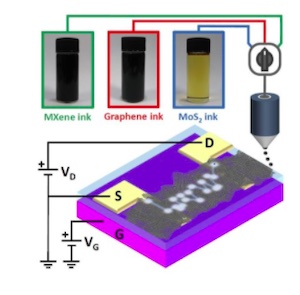
The team investigated three typical types of 2D materials: graphene (a ‘semimetal’ built from a single layer of carbon atoms), molybdenum disulphide (or MoS2, a ‘semiconductor’) and titanium carbide MXene (or Ti3C2, a metal) and mapped how the behaviour of the electrical charge transport changed under these different conditions.
These future devices could one day replace invasive procedures, such as implanting brain electrodes to monitor degenerative conditions that affect the nervous system. Electrodes can only be implanted on a temporary basis, and are uncomfortable for the patient, whereas a flexible device made of biocompatible 2D materials could be integrated with the brain and provide constant monitoring.
Lead researcher Dr Felice Torrisi, from the Department of Chemistry at Imperial, said: “Our results have a huge impact on the way we understand the transport through networks of two-dimensional materials, enabling not only the controlled design and engineering of future printed electronics based on 2D materials, but also new types of flexible electronic devices.
“For example, our work paves the way to reliable wearable devices suitable for biomedical applications, such as the remote monitoring of patients, or bio-implantable devices for long-term monitoring of degenerative diseases or healing processes.”
Other potential healthcare applications include wearable devices for monitoring healthcare – devices like fitness watches, but more integrated with the body, providing sufficiently accurate data to allow doctors to monitor patients without bringing them into hospital for tests.
Optimal designs
The relationships the team discovered between 2D material type and the controls on electrical charge transport will help other researchers design printed and flexible 2D material devices with the properties they desire, based on how they need the electrical charge to act.
They could also reveal how to design entirely new types of electrical components impossible using silicon chips, such as transparent components or ones that modify and transmit light in new ways.
Co-author Professor Renato Gonnelli, from the Politecnico di Torino, Italy, said: “The fundamental understanding of how the electrons are transported through networks of 2D materials underpins the way we manufacture printed electronic components. By identifying the mechanisms responsible for such electronic transport, we will be able to achieve the optimum design of high-performance printed electronics.”
Co-first author Adrees Arbab, from the Department of Chemistry at Imperial and the Cambridge Graphene Centre, said: “In addition, our study could unleash the new electronic and optoelectronic devices exploiting the innovative properties of graphene and other 2D materials, such as incredibly high mobility, optical transparency, and mechanical strength.”
Read the original article, here.
Share on:


Testimonial
"We’re proud to call I-Connect007 a trusted partner. Their innovative approach and industry insight made our podcast collaboration a success by connecting us with the right audience and delivering real results."
Julia McCaffrey - NCAB GroupSuggested Items
NEDME 2025 Draws Strong Northwest Crowd, Builds on Tradition of Regional Collaboration
10/31/2025 | NEDMEThe NW Electronics Design & Manufacturing Expo (NEDME) 2025 once again brought together the Pacific Northwest community for a full day of learning, networking, and industry connections.
Keysight Advances Quantum Engineering with New System-Level Simulation Solution
10/30/2025 | BUSINESS WIREKeysight Technologies, Inc. announced the release of Quantum System Analysis, a breakthrough Electronic Design Automation (EDA) solution that enables quantum engineers to simulate and optimize quantum systems at the system level.
WestDev Announces Advanced Thermal Analysis Integration for Pulsonix PCB Design Suite
10/29/2025 | WestDev Ltd.Pulsonix, the industry-leading PCB design software from WestDev Ltd., announced a major enhancement to its design ecosystem: a direct interface between Pulsonix and ADAM Research's TRM (Thermal Risk Management) analysis software.
Industry Veteran Dr. Helen Song Joins Celera Semiconductor to Lead Product Design
10/28/2025 | PRNewswireCelera Semiconductor, the analog industry leader using AI to automate the entire product development flow, today announced that Dr. Helen Song has joined the company as vice president of Product Design.
Mapping the EV Landscape: Markets, Platforms, and Powertrains
10/28/2025 | Stanton Rak, SF Rak Companye-Mobility is the defining transformation of 21st-century transportation. As legacy OEMs, startups, and governments race to electrify vehicle fleets, the landscape of e-Mobility is expanding into previously unimaginable territory. But with innovation comes complexity, and with complexity, a need for systems that are not only high-performing but also reliably engineered for the long haul. Understanding the diversity and scale of the EV marketplace is essential to grasping the reliability challenges ahead.