


 Beyond the Board: Early Engagement Means Faster Prototyping for Defense Programs
 Defense Speak Interpreted: The Autonomous Plane Battle—Skyborg Vs. Loyal Wingman
 American Made Advocacy: Congress Back from Break With Work To Do


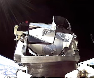
DARPA Kicks Off Program to Explore Space-Based Manufacturing
March 28, 2022 | DARPAEstimated reading time: 2 minutes
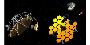
DARPA’s Novel Orbital Moon Manufacturing, Materials, and Mass Efficient Design (NOM4D) program is underway with eight industry and university research teams on contract. The selected teams are tasked to provide foundational proofs of concept in materials science, manufacturing, and design technologies to enable production of future space structures on orbit without the volume constraints imposed by launch. The vision is to ferry raw materials from Earth and collect lunar materials for on-orbit manufacturing. The NOM4D program does not involve building any structures on the surface of the moon. All manufacturing would be done in orbital construction facilities and the results utilized in orbital applications.
“Current space systems are all designed, built, and tested on Earth before being launched into a stable orbit and deployed to their final operational configuration,” said Bill Carter NOM4D program manager in DARPA’s Defense Sciences Office. “These constraints are particularly acute for large structures such as solar arrays, antennas and optical systems, where size is critical to performance. NOM4D aims to enable a new paradigm where future structures that support DoD space systems are built off-Earth using designs optimized for the space environment, shedding launch constraints. This would enable enhanced capability, improved robustness, operation in higher orbits, and future cislunar applications.”
For NOM4D, performers won’t be launching raw materials into space, collecting lunar samples or building structures on orbit. Any orbital experimentation would happen in potential follow-on efforts.
The following research teams are on contract to pursue a variety of challenges focused on two areas listed below:
1. In-space materials and manufacturing
- HRL Laboratories, LLC, Malibu, California, will be developing new die-less fabrication processes to make orbital mechanical elements and bonded structures on-orbit.
- University of Florida, Gainesville, Florida, will develop predictive material and correlative process models to enable on-orbit use of laser forming.
- University of Illinois Urbana-Champaign, Champaign, Illinois, is working to develop a high precision in-space composite forming process utilizing self-energized frontal polymerization.
- Physical Sciences, Inc., Andover, Massachusetts, will develop continuous fabrication of regolith-derived, glass-ceramic mechanical structures for use in large-scale orbital applications.
- Teledyne Scientific Company, LLC, Thousand Oaks, California, will build a comprehensive materials properties database of additive-modified regolith for use in controlled thermal expansion precision orbital structures.
2. Mass-efficient designs for in-space manufacturing
- University of Michigan, Ann Arbor, Michigan, will explore new design approaches to mass-efficient, high- precision, stable and resilient space structures based on metamaterial and metadamping concepts.
- Opterus Research and Development, Inc., Loveland, Colorado, will develop designs for extreme mass efficient large-scale structures optimized for resiliency and mobility.
- California Institute of Technology, Pasadena, California, will design novel tension and bending hybrid architectures and structural components with highly anisotropic mechanical response.
During Phase 1, program performers are tasked to meet stringent structural efficiency targets supporting a megawatt-class solar array. In Phase 2, teams are tasked to increase mass efficiency and demonstrate precision manufacturing for radio frequency (RF) reflectors. In the final phase, performers are tasked to demonstrate precision for infrared (IR) reflectors.
“Assuming current space technology trends continue, in 10-20 years we expect to see advances that will enable DoD to take full advantage of the NOM4D-developed technologies and capabilities,” Carter said. “This includes robotic manipulation sufficient to enable assembly of large structures from NOM4D-manufactured components, enhanced on-orbit mobility, and routine re-fueling of on-orbit assets. We also anticipate several other advantages, including more affordable space access and launch costs in LEO [low-earth orbit], GEO [geosynchronous orbit], cislunar space, and beyond.”
Share on:


Testimonial
"Advertising in PCB007 Magazine has been a great way to showcase our bare board testers to the right audience. The I-Connect007 team makes the process smooth and professional. We’re proud to be featured in such a trusted publication."
Klaus Koziol - atgSuggested Items
ASE, Analog Devices Announce Strategic Collaboration
10/21/2025 | BUSINESS WIREASE Technology Holding Co., Ltd., and Analog Devices, Inc., announced strategic joint efforts in Penang, Malaysia with the signing of a binding Memorandum of Understanding.
Flex Sites in Brazil and Mexico Recognized as Manufacturing Leaders by the Association for Manufacturing Excellence
10/21/2025 | PRNewswireFlex announced that its sites in Manaus, Brazil, and our plastics operations in Guadalajara, Mexico, each received an Excellence Award from the Association for Manufacturing Excellence (AME), demonstrating global leadership in continuous improvement and operational excellence.
Global Electronics Association Releases Fall Schedule of Instructor-led Courses
10/20/2025 | Corey Lynn, Global Electronics AssociationWhether you’re looking to enhance your PCB design skills, explore advanced packaging technologies, or deepen your understanding of reliability, these Global Electronics Association courses deliver high-impact learning from the best in the industry. Here are a few starting this week.
Fabrinet Announces Retirement of Founder and Chairman Tom Mitchell After 25 Years of Visionary Leadership
10/20/2025 | FabrinetFabrinet, a leading provider of advanced optical packaging and precision optical, electro-mechanical and electronic manufacturing services to original equipment manufacturers of complex products, announced the retirement of company founder and Chairman, David T. (Tom) Mitchell, after 25 years of visionary leadership.
Marcy’s Musings: The Legislative Outlook—Helping or Hurting?
10/20/2025 | Marcy LaRont -- Column: Marcy's MusingsJust before we were ready to publish our October issue of PCB007 Magazine, some breaking news from the White House, unfortunately (but perfectly) parlayed into why the topic of this month’s issue has been so important to cover in great depth.